SLUSEA4D June 2021 – August 2022 TPS62932 , TPS62933 , TPS62933F , TPS62933O , TPS62933P
PRODUCTION DATA
- 1 Features
- 2 Applications
- 3 Description
- 4 Revision History
- 5 Description (continued)
- 6 Device Comparison Table
- 7 Pin Configuration and Functions
- 8 Specifications
-
9 Detailed Description
- 9.1 Overview
- 9.2 Functional Block Diagram
- 9.3
Feature Description
- 9.3.1 Fixed Frequency Peak Current Mode
- 9.3.2 Pulse Frequency Modulation
- 9.3.3 Voltage Reference
- 9.3.4 Output Voltage Setting
- 9.3.5 Switching Frequency Selection
- 9.3.6 Enable and Adjusting Undervoltage Lockout
- 9.3.7 External Soft Start and Prebiased Soft Start
- 9.3.8 Power Good
- 9.3.9 Minimum On Time, Minimum Off Time, and Frequency Foldback
- 9.3.10 Frequency Spread Spectrum
- 9.3.11 Overvoltage Protection
- 9.3.12 Overcurrent and Undervoltage Protection
- 9.3.13 Thermal Shutdown
- 9.4 Device Functional Modes
-
10Application and Implementation
- 10.1 Application Information
- 10.2
Typical Application
- 10.2.1 Design Requirements
- 10.2.2
Detailed Design Procedure
- 10.2.2.1 Custom Design With WEBENCH® Tools
- 10.2.2.2 Output Voltage Resistors Selection
- 10.2.2.3 Choosing Switching Frequency
- 10.2.2.4 Soft-Start Capacitor Selection
- 10.2.2.5 Bootstrap Capacitor Selection
- 10.2.2.6 Undervoltage Lockout Setpoint
- 10.2.2.7 Output Inductor Selection
- 10.2.2.8 Output Capacitor Selection
- 10.2.2.9 Input Capacitor Selection
- 10.2.2.10 Feedforward Capacitor CFF Selection
- 10.2.2.11 Maximum Ambient Temperature
- 10.2.3 Application Curves
- 10.3 What to Do and What Not to Do
- 11Power Supply Recommendations
- 12Layout
- 13Device and Documentation Support
- 14Mechanical, Packaging, and Orderable Information
Package Options
Mechanical Data (Package|Pins)
- DRL|8
Thermal pad, mechanical data (Package|Pins)
Orderable Information
10.2.2.2 Output Voltage Resistors Selection
The output voltage is set with a resistor divider from the output node to the FB pin. TI recommends using 1% tolerance or better divider resistors. Referring to the application schematic of Figure 10-1, start with 10.2 kΩ for R7 and use Equation 14 to calculate R6 = 53.6 kΩ. To improve efficiency at light loads, consider using larger value resistors. If the values are too high, the converter is more susceptible to noise and voltage errors from the FB input leakage current are noticeable.
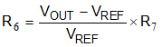
Table 10-2 shows the recommended components value for common output voltages.