SLVS696D October   2008  – April 2020 TPS63030 , TPS63031

PRODUCTION DATA.  

  1. Features
  2. Applications
  3. Description
    1.     Device Images
      1.      Typical Application Schematic
      2.      Efficiency versus Output Current
  4. Revision History
  5. Output Voltage Options
  6. Pin Configuration and Functions
    1.     Pin Functions
  7. Specifications
    1. 7.1 Absolute Maximum Ratings
    2. 7.2 ESD Ratings
    3. 7.3 Recommended Operating Conditions
    4. 7.4 Thermal Information
    5. 7.5 Electrical Characteristics
    6. 7.6 Typical Characteristics
  8. Detailed Description
    1. 8.1 Overview
    2. 8.2 Functional Block Diagrams
    3. 8.3 Feature Description
      1. 8.3.1 Device Enable
      2. 8.3.2 Undervoltage Lockout
      3. 8.3.3 Overtemperature Protection
    4. 8.4 Device Functional Modes
      1. 8.4.1 Soft Start and Short Circuit Protection
      2. 8.4.2 Buck-Boost Operation
      3. 8.4.3 Power-Save Mode and Synchronization
  9. Application and Implementation
    1. 9.1 Application Information
    2. 9.2 Typical Application
      1. 9.2.1 Design Requirements
      2. 9.2.2 Detailed Design Procedure
        1. 9.2.2.1 Programming the Output Voltage
        2. 9.2.2.2 Inductor Selection
        3. 9.2.2.3 Capacitor Selection
          1. 9.2.2.3.1 Input Capacitor
          2. 9.2.2.3.2 Bypass Capacitor
          3. 9.2.2.3.3 Output Capacitor
      3. 9.2.3 Application Curves
  10. 10Power Supply Recommendations
  11. 11Layout
    1. 11.1 Layout Guidelines
    2. 11.2 Layout Example
    3. 11.3 Thermal Considerations
  12. 12Device and Documentation Support
    1. 12.1 Device Support
      1. 12.1.1 Third-Party Products Disclaimer
    2. 12.2 Documentation Support
      1. 12.2.1 Related Documentation
    3. 12.3 Related Links
    4. 12.4 Support Resources
    5. 12.5 Trademarks
    6. 12.6 Electrostatic Discharge Caution
    7. 12.7 Glossary
  13. 13Mechanical, Packaging, and Orderable Information

Package Options

Mechanical Data (Package|Pins)
Thermal pad, mechanical data (Package|Pins)
Orderable Information

Pin Configuration and Functions

DSK Package
10-Pin VSON
Top View
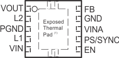
TPS63030 TPS63031 po_lvs696_ETP.gif
The exposed thermal pad is connected to PGND.

Pin Functions

PIN I/O DESCRIPTION
NAME NO.
EN 6 IN Enable input (1 enabled, 0 disabled)
FB 10 IN Voltage feedback of adjustable versions, must be connected to VOUT on fixed output voltage versions
GND 9 Control / logic ground
L1 4 IN Connection for inductor
L2 2 IN Connection for inductor
PGND 3 Power ground
PS/SYNC 7 IN Enable / disable power save mode (1 disabled, 0 enabled, clock signal for synchronization)
VIN 5 IN Supply voltage for power stage
VINA 8 IN Supply voltage for control stage
VOUT 1 OUT Buck-boost converter output
Exposed Thermal Pad The exposed thermal pad is connected to PGND.