SLVS670L June 2006 – May 2018 TPS65023 , TPS65023B
PRODUCTION DATA.
- 1 Features
- 2 Applications
- 3 Description
- 4 Revision History
- 5 Pin Configuration and Functions
-
6 Specifications
- 6.1 Absolute Maximum Ratings
- 6.2 ESD Ratings
- 6.3 Recommended Operating Conditions
- 6.4 Thermal Information
- 6.5 Electrical Characteristics
- 6.6 Electrical Characteristics: Supply Pins VCC, VINDCDC1, VINDCDC2, VINDCDC3
- 6.7 Electrical Characteristics: Supply Pins VBACKUP, VSYSIN, VRTC, VINLDO
- 6.8 Electrical Characteristics: VDCDC1 Step-Down Converter
- 6.9 Electrical Characteristics: VDCDC2 Step-Down Converter
- 6.10 Electrical Characteristics: VDCDC3 Step-Down Converter
- 6.11 I2C Timing Requirements for TPS65023B
- 6.12 Typical Characteristics
-
7 Detailed Description
- 7.1 Overview
- 7.2 Functional Block Diagram
- 7.3
Feature Description
- 7.3.1 VRTC Output and Operation With or Without Backup Battery
- 7.3.2 Step-Down Converters, VDCDC1, VDCDC2, and VDCDC3
- 7.3.3 Power Save Mode Operation
- 7.3.4 Low Ripple Mode
- 7.3.5 Soft-Start
- 7.3.6 100% Duty Cycle Low Dropout Operation
- 7.3.7 Active Discharge When Disabled
- 7.3.8 Power-Good Monitoring
- 7.3.9 Low-Dropout Voltage Regulators
- 7.3.10 Undervoltage Lockout
- 7.3.11 Power-Up Sequencing
- 7.4 Device Functional Modes
- 7.5 Programming
- 7.6
Register Maps
- 7.6.1 VERSION Register Address: 00h (Read Only)
- 7.6.2 PGOODZ Register Address: 01h (Read Only)
- 7.6.3 MASK Register Address: 02h (Read and Write), Default Value: C0h
- 7.6.4 REG_CTRL Register Address: 03h (Read and Write), Default Value: FFh
- 7.6.5 CON_CTRL Register Address: 04h (Read and Write), Default Value: B1h
- 7.6.6 CON_CTRL2 Register Address: 05h (Read and Write), Default Value: 40h
- 7.6.7 DEFCORE Register Address: 06h (Read and Write), Default Value: 14h/1Eh
- 7.6.8 DEFSLEW Register Address: 07h (Read and Write), Default Value: 06h
- 7.6.9 LDO_CTRL Register Address: 08h (Read and Write), Default Value: Set with DEFLDO1 and DEFLDO2
- 8 Application and Implementation
- 9 Power Supply Recommendations
- 10Layout
- 11Device and Documentation Support
- 12Mechanical, Packaging, and Orderable Information
Package Options
Refer to the PDF data sheet for device specific package drawings
Mechanical Data (Package|Pins)
- RSB|40
Thermal pad, mechanical data (Package|Pins)
- RSB|40
Orderable Information
8.2.3 Application Curves
Graphs were taken using the EVM with the following inductor and output capacitor combinations:
| CONVERTER | INDUCTOR | OUTPUT CAPACITOR | OUTPUT CAPACITOR VALUE |
|---|---|---|---|
| VDCDC1 | VLCF4020-2R2 | C2012X5R0J106M | 2 × 10 μF |
| VDCDC2 | VLCF4020-2R2 | C2012X5R0J106M | 2 × 10 μF |
| VDCDC3 | VLF4012AT-2R2M1R5 | C2012X5R0J106M | 2 × 10 μF |
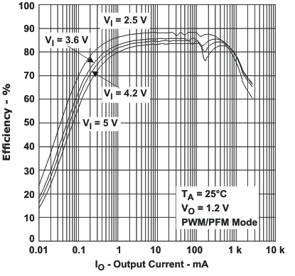
 Figure 42. DCDC1 Efficiency
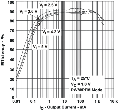
 Figure 44. DCDC3 Efficiency
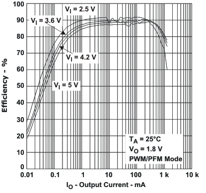
 Figure 43. DCDC2 Efficiency