SLVS670L June 2006 – May 2018 TPS65023 , TPS65023B
PRODUCTION DATA.
- 1 Features
- 2 Applications
- 3 Description
- 4 Revision History
- 5 Pin Configuration and Functions
-
6 Specifications
- 6.1 Absolute Maximum Ratings
- 6.2 ESD Ratings
- 6.3 Recommended Operating Conditions
- 6.4 Thermal Information
- 6.5 Electrical Characteristics
- 6.6 Electrical Characteristics: Supply Pins VCC, VINDCDC1, VINDCDC2, VINDCDC3
- 6.7 Electrical Characteristics: Supply Pins VBACKUP, VSYSIN, VRTC, VINLDO
- 6.8 Electrical Characteristics: VDCDC1 Step-Down Converter
- 6.9 Electrical Characteristics: VDCDC2 Step-Down Converter
- 6.10 Electrical Characteristics: VDCDC3 Step-Down Converter
- 6.11 I2C Timing Requirements for TPS65023B
- 6.12 Typical Characteristics
-
7 Detailed Description
- 7.1 Overview
- 7.2 Functional Block Diagram
- 7.3
Feature Description
- 7.3.1 VRTC Output and Operation With or Without Backup Battery
- 7.3.2 Step-Down Converters, VDCDC1, VDCDC2, and VDCDC3
- 7.3.3 Power Save Mode Operation
- 7.3.4 Low Ripple Mode
- 7.3.5 Soft-Start
- 7.3.6 100% Duty Cycle Low Dropout Operation
- 7.3.7 Active Discharge When Disabled
- 7.3.8 Power-Good Monitoring
- 7.3.9 Low-Dropout Voltage Regulators
- 7.3.10 Undervoltage Lockout
- 7.3.11 Power-Up Sequencing
- 7.4 Device Functional Modes
- 7.5 Programming
- 7.6
Register Maps
- 7.6.1 VERSION Register Address: 00h (Read Only)
- 7.6.2 PGOODZ Register Address: 01h (Read Only)
- 7.6.3 MASK Register Address: 02h (Read and Write), Default Value: C0h
- 7.6.4 REG_CTRL Register Address: 03h (Read and Write), Default Value: FFh
- 7.6.5 CON_CTRL Register Address: 04h (Read and Write), Default Value: B1h
- 7.6.6 CON_CTRL2 Register Address: 05h (Read and Write), Default Value: 40h
- 7.6.7 DEFCORE Register Address: 06h (Read and Write), Default Value: 14h/1Eh
- 7.6.8 DEFSLEW Register Address: 07h (Read and Write), Default Value: 06h
- 7.6.9 LDO_CTRL Register Address: 08h (Read and Write), Default Value: Set with DEFLDO1 and DEFLDO2
- 8 Application and Implementation
- 9 Power Supply Recommendations
- 10Layout
- 11Device and Documentation Support
- 12Mechanical, Packaging, and Orderable Information
Package Options
Refer to the PDF data sheet for device specific package drawings
Mechanical Data (Package|Pins)
- RSB|40
Thermal pad, mechanical data (Package|Pins)
- RSB|40
Orderable Information
3 Description
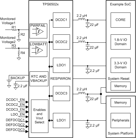
The TPS65023x device is an integrated power management IC for applications powered by one
Li-Ion or Li-Polymer cell, which require multiple power rails. The TPS65023x provides three highly efficient, step-down converters targeted at providing the core voltage, peripheral, I/O, and memory rails in a processor-based system. The core converter allows for on-the-fly voltage changes through serial interface, allowing the system to implement dynamic power savings. All three step-down converters enter a low-power mode at light load for maximum efficiency across the widest possible range of load currents.
The TPS65023x also integrates two general-purpose 200-mA LDO voltage regulators, which are enabled with an external input pin. Each LDO operates with an input voltage range from 1.5 V to 6.5 V, thus allowing them to be supplied from one of the step-down converters or directly from the battery. The default output voltage of the LDOs can be digitally set to 4 different voltage combinations using the DEFLDO1 and DEFLDO2 pins. The serial interface can be used for dynamic voltage scaling, masking interrupts, or for disabling or enabling and setting the LDO output voltages. The interface is compatible with both the fast and standard mode I2C specifications, allowing transfers at up to 400 kHz. The TPS65023x is available in a 40-pin WQFN package, and operates over a free-air temperature of –40°C to 85°C.
Device Information(1)
| PART NUMBER | PACKAGE | BODY SIZE (NOM) |
|---|---|---|
| TPS65023 | WQFN (40) | 5.00 mm × 5.00 mm |
| TPS65023B |
- For all available packages, see the orderable addendum at the end of the data sheet.
Simplified Schematic
