SLVS774C June 2007 – January 2016 TPS650240 , TPS650241 , TPS650242 , TPS650243 , TPS650244 , TPS650245
PRODUCTION DATA.
- 1 Features
- 2 Applications
- 3 Description
- 4 Revision History
- 5 Description (continued)
- 6 Pin Configuration and Functions
-
7 Specifications
- 7.1 Absolute Maximum Ratings
- 7.2 ESD Ratings
- 7.3 Recommended Operating Conditions
- 7.4 Thermal Information
- 7.5 Electrical Characteristics: Control Signals and Supply Pins
- 7.6 Electrical Characteristics: VDCDC1 Step-Down Converter
- 7.7 Electrical Characteristics: VDCDC2 Step-Down Converter
- 7.8 Electrical Characteristics: VDCDC3 Step-Down Converter
- 7.9 Electrical Characteristics: General
- 7.10 Typical Characteristics
- 8 Detailed Description
- 9 Application and Implementation
- 10Power Supply Recommendations
- 11Layout
- 12Device and Documentation Support
- 13Mechanical, Packaging, and Orderable Information
Package Options
Mechanical Data (Package|Pins)
- RHB|32
Thermal pad, mechanical data (Package|Pins)
- RHB|32
Orderable Information
9 Application and Implementation
NOTE
Information in the following applications sections is not part of the TI component specification, and TI does not warrant its accuracy or completeness. TI’s customers are responsible for determining suitability of components for their purposes. Customers should validate and test their design implementation to confirm system functionality.
9.1 Application Information
9.1.1 Output Voltage Selection
The DEFDCDC1, DEFDCDC2, and DEFDCDC3 pins are used to set the output voltage for each step-down converter. See Table 3 for the default voltages if the pins are pulled to GND or to VCC.
Table 3. Voltage Options
| PIN | LEVEL | DEFAULT OUTPUT VOLTAGE | |
|---|---|---|---|
| DEFDCDC1 | All versions | VCC | 3.3 V |
| GND | 2.80 V | ||
| DEFDCDC2 | All versions | VCC | 2.5 V |
| GND | 1.8 V | ||
| DEFDCDC3 | TPS650240 | VCC | 1.3 V |
| GND | 1.0 V | ||
| TPS650241 | VCC | 1.375 V | |
| GND | 0.9 V | ||
| TPS650242 | VCC | 1.5 V | |
| GND | 1.0 V | ||
| TPS650243 | VCC | 1.2 V | |
| GND | 1.0 V | ||
| TPS650244 | VCC | 1.6 V | |
| GND | 1.55 V | ||
| TPS650245 | VCC | 1.1 V | |
| GND | 0.9 V | ||
If a different voltage is needed, an external resistor divider can be added to the DEFDCDC1 or DEFDCDC2 pin as shown in Figure 18.
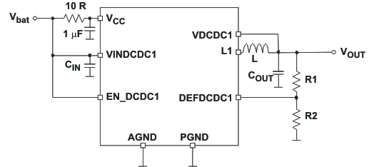 Figure 18. External Resistor Divider Diagram
When a resistor divider is connected to DEFDCDC1 or DEFDCDC2, the output voltage can be set from 0.6 V up to the input voltage Vbat. The total resistance (R1 + R2) of the voltage divider must be kept in the 1-MΩ range to maintain a high efficiency at light load. Detailed calculations for selecting these resistance values are presented in Equation 8 and Equation 9, where VDEFDCDCx = 0.6 V.


9.1.2 Voltage Change on VDCDC3
The output voltage of VDCDC3 can be changed during operation from, for example, 1.0 V to 1.3 V (TPS650240), and back. While the output voltage at VDCDC1 and VDCDC2 is fixed after the device exits undervoltage lockout (UVLO), the status of the DEFDCDC3 pin is sensed during operation and the voltage is changed as soon as the logic level on this pin changes from low to high or vice versa. Therefore it is not possible to connect a resistor divider to DEFDCDC3 and set a voltage different from the predefined voltages.
9.1.3 Vdd_alive Output
The Vdd_alive LDO is typically connected to a logic input of an external device or application processor, and is capable of providing an output voltage of 1.2 V at 30 mA. For the TPS650245, the output voltage for vdd_alive is set to 1.1 V. TI recommends adding a capacitor of 2.2 μF minimum to the Vdd_alive pin. The LDO can be disabled by pulling the EN_Vdd_alive pin to GND.
9.1.4 LDO1 and LDO2
The LDOs in the TPS65024x are general-purpose LDOs which are stable using ceramics capacitors. The minimum output capacitance required is 2.2 μF. The LDOs output voltage can be changed to different voltages between 1.0 V and Vin using an external resistor divider. Therefore they can also be used as general-purpose LDOs in the application. The supply voltage for the LDOs needs to be connected to the VINLDO pin, giving the flexibility to connect the lowest voltage available in the system and therefore providing the highest efficiency.
The total resistance (R5 + R6) of the voltage divider must be kept in the 1-MΩ range to maintain high efficiency at light load. Detailed calculations for selecting these resistance values are presented in Equation 10 and Equation 11, where VFBLDOx= 1.0 V.


9.1.5 VCC Filter
An RC filter connected at the VCC input is recommended to prevent noise from entering the internal supply used for the bandgap and other analog circuitry. A typical value of 1 Ω and 1 μF is used to filter the switching spikes, generated by the DC–DC converters. A larger resistor than 10 Ω must not be used because the current into VCC of up to 2.5 mA causes a voltage drop at the resistor causing the undervoltage lockout circuitry connected at VCC internally to switch off too early.
9.2 Typical Applications
9.2.1 Typical Configuration for the Samsung Processor S3C6400-533MHz
The typical configuration for the Samsung processor S3C6400-533-MHz is shown in Figure 19. This application uses only the default output values for the step-down converters, specifying regulation targets with high and low logic on the DEFDCDCx pins.
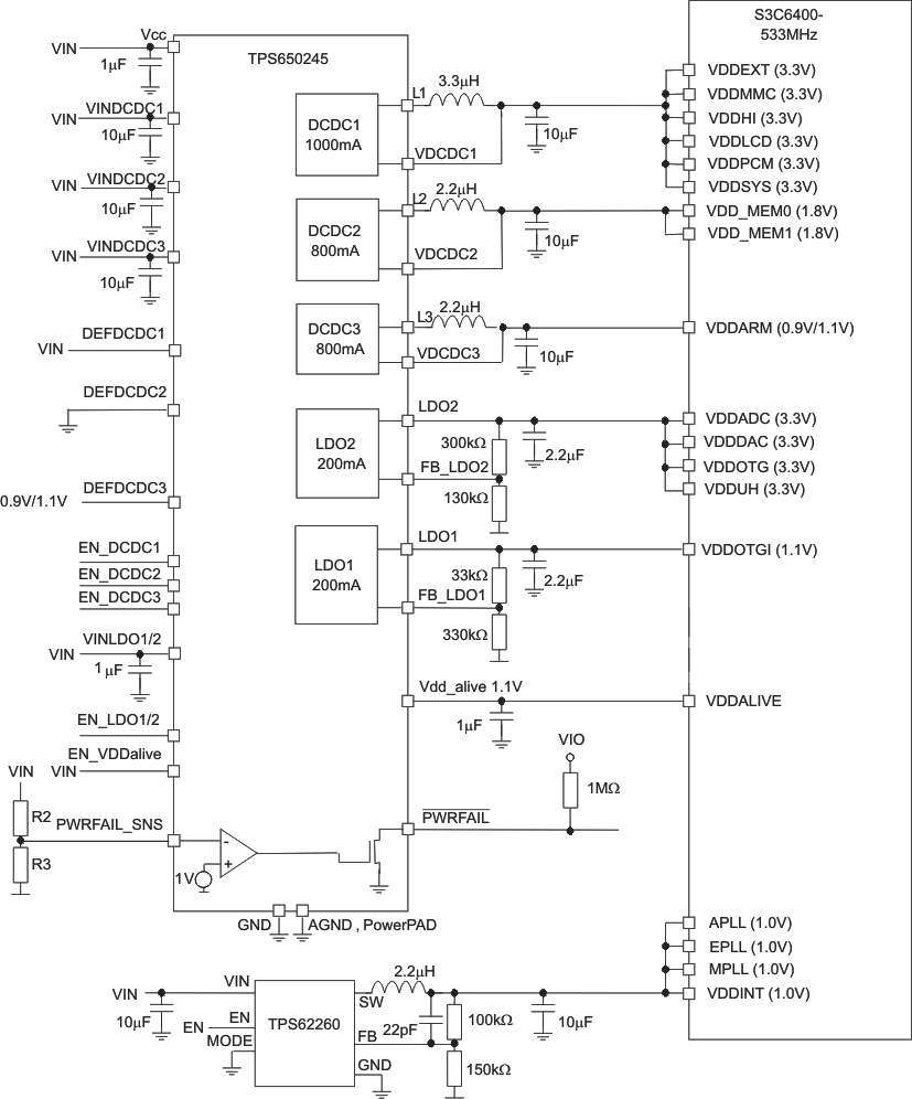 Figure 19. Samsung Processor Configuration
9.2.1.1 Design Requirements
Each step-down converter requires an input decoupling capacitor, an output inductor, and an output filter capacitor. Desired output voltages must be configured through appropriate DEFDCDCx voltages, and all components must be selected to handle the maximum output currents, as well as any transient or ripple specifications that may be required for the expected loads.
The LDOs must have a decoupling capacitor on the input voltage pin, and a dedicated filter capacitor on each LDO output.
9.2.1.2 Detailed Design Procedure
9.2.1.2.1 Inductor Selection for the DC-DC Converters
The three converters operate with 2.2-µH output inductors. Larger or smaller inductor values can be used to optimize performance of the device for specific conditions. The selected inductor has to be rated for its DC resistance and saturation current. The DC resistance of the inductor influences directly the efficiency of the converter. Therefore, an inductor with the lowest DC resistance must be selected for the highest efficiency.
For a fast transient response, a 2.2-μH inductor in combination with a 22-μF output capacitor is recommended. For an output voltage above 2.8 V, an inductor value of 3.3 μH minimum is required. Lower values result in an increased output voltage ripple in PFM mode. The minimum inductor value is 1.5 μH, but an output capacitor of 22 μF minimum is needed in this case.
Equation 12 calculates the maximum inductor current under static load conditions. The saturation current of the inductor must be rated higher than the maximum inductor current as calculated with Equation 12. This is recommended because during heavy-load transient, the inductor current rises above the calculated value.

where
- f = Switching frequency (2.25 MHz typical)
- L = Inductor value
- ΔIL = Peak-to-peak inductor ripple current
- ILmax = Maximum inductor current
The highest inductor current occurs at maximum Vin.
Open-core inductors have a soft saturation characteristic and they can usually handle higher inductor currents versus a comparable shielded inductor.
A more conservative approach is to select the inductor current rating just for the maximum switch current of the corresponding converter. Consideration must be given to the difference in the core material from inductor to inductor which has an impact on efficiency especially at high switching frequencies.
9.2.1.2.2 Output Capacitor Selection
The advanced fast response voltage mode control scheme of the inductive converters implemented in the TPS65024x allows the use of small ceramic capacitors with a typical value of 10 µF for each converter, without having large output voltage under and overshoots during heavy load transients. Ceramic capacitors having low ESR values have the lowest output voltage ripple and are recommended.
If ceramic output capacitors are used, the capacitor RMS ripple current rating will always meet the application requirements. For completeness, the RMS ripple current is calculated as Equation 13:

At nominal load current the inductive converters operate in PWM mode and the overall output voltage ripple is the sum of the voltage spike caused by the output capacitor ESR plus the voltage ripple caused by charging and discharging the output capacitor:

where
- the highest output voltage ripple occurs at the highest input voltage, Vin
At light-load currents the converters operate in power save mode and output voltage ripple is dependent on the output capacitor value. The output voltage ripple is set by the internal comparator delay and the external capacitor. Typical output voltage ripple is less than 1% of the nominal output voltage.
9.2.1.2.3 Input Capacitor Selection
Because of the nature of the buck converter having a pulsating input current, a low ESR input capacitor is required for best input voltage filtering and minimizing interference with other circuits caused by high input voltage spikes. Each DC–DC converter requires a 10-μF ceramic input capacitor on its input pin VINDCDCx. The input capacitor can be increased without any limit for better input voltage filtering. The VCC pin must be separated from the input for the DC–DC converters. A filter resistor of up to 10 Ω and a 1-μF capacitor must be used for decoupling the VCC pin from switching noise.
NOTE
The filter resistor may affect the UVLO threshold since up to 3 mA can flow through this resistor into the VCC pin when all converters are running in PWM mode.
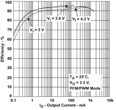
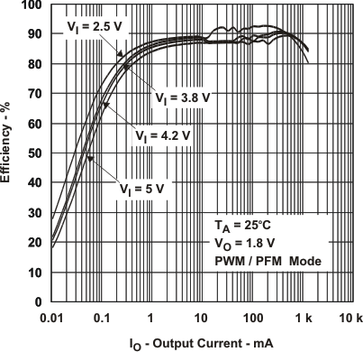
9.2.1.3 Application Curves
9.2.2 Typical Configuration for the Titan 2 Processor
The typical configuration for the Titan processor is shown in Figure 22. This application highlights the ability to increase the voltage on DCDC3 by using a single external resistor.
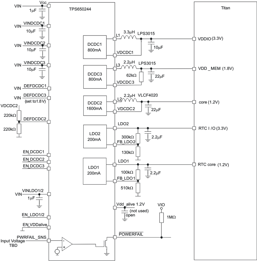 Figure 22. Titan Processor Configuration
9.2.2.1 Design Requirements
Each step-down converter requires an input decoupling capacitor, an output inductor, and an output filter capacitor. Desired output voltages must be configured through appropriate DEFDCDCx voltages, and all components must be selected to handle the maximum output currents, as well as any transient or ripple specifications that may be required for the expected loads.
The LDOs must have a decoupling capacitor on the input voltage pin, and a dedicated filter capacitor on each LDO output.
9.2.2.2 Detailed Design Procedure
Refer to the Samsung Processor Detailed Design Procedure for full design procedure details.
As only DCDC2 on the TPS650244 is capable of supporting a sufficient core current up to 1.6 A, a resistive divider is first implemented on DEFDCDC2 to produce this required 1.2-V rail. DCDC3 is then modified to support the memory voltage of 1.8 V. As DCDC3 cannot support 1.8 V from a default configuration, the output voltage is first programmed to a lower value, in this case 1.6 V, by setting DEFDCDC3 = HIGH. Even though DCDC3 does not support an external resistor divider on DEFDCDC3, it can still be tricked into regulating a higher output voltage of 1.8 V by presenting the VDCDC3 feedback pin with 200 mV less than the original target of 1.6 V. The internal resistance at VDCDC3 when programmed to 1.6 V is 480 kΩ, so the external resistance needed to drop 200 mV within the feedback path and increase the output voltage from 1.6 V to 1.8 V is 60 kΩ (62 kΩ).