SLVSBO6B January 2013 – July 2015 TPS65090
PRODUCTION DATA.
- 1 Features
- 2 Applications
- 3 Description
- 4 Revision History
- 5 Pin Configuration and Functions
-
6 Specifications
- 6.1 Absolute Maximum Ratings
- 6.2 ESD Ratings
- 6.3 Recommended Operating Conditions
- 6.4 Thermal Information
- 6.5 Electrical Characteristics - Power Path Control
- 6.6 Electrical Characteristics - Charger
- 6.7 Electrical Characteristics - DC-DC Converters
- 6.8 Electrical Characteristics - Linear Regulators
- 6.9 Electrical Characteristics - Load Switches
- 6.10 Electrical Characteristics - Control
- 6.11 Timing Requirements - I2C Interface
- 6.12 Typical Characteristics
- 7 Detailed Description
-
8 Application and Implementation
- 8.1 Application Information
- 8.2
Typical Applications
- 8.2.1
Front-End PMU Application
- 8.2.1.1 Design Requirements
- 8.2.1.2
Detailed Design Procedure
- 8.2.1.2.1 Programming the Converter or Charger Output Voltage
- 8.2.1.2.2 Programming Input DPM Current and Charge Current
- 8.2.1.2.3 Output Filter Design (Inductor and Output Capacitor)
- 8.2.1.2.4 Inductor Selection
- 8.2.1.2.5 Capacitor Selection
- 8.2.1.2.6 Charger Battery Temperature Sensing
- 8.2.1.2.7 Reverse Voltage Protection
- 8.2.1.2.8 AC Switches
- 8.2.1.2.9 Battery Switches
- 8.2.1.3 Application Curves
- 8.2.2 DC-DC Converters
- 8.2.3 Charger
- 8.2.1
Front-End PMU Application
- 9 Power Supply Recommendations
- 10Layout
- 11Device and Documentation Support
- 12Mechanical, Packaging, and Orderable Information
Package Options
Mechanical Data (Package|Pins)
- RVN|100
Thermal pad, mechanical data (Package|Pins)
- RVN|100
Orderable Information
6 Specifications
6.1 Absolute Maximum Ratings
over operating free-air temperature range (unless otherwise noted)(1)| MIN | MAX | UNIT | ||
|---|---|---|---|---|
| POWER PATH CONTROL | ||||
| Voltage(2) | VAC, VACS | –0.3 | 30 | V |
| ACP, ACN, ACS, BATG | –0.3 | 20 | ||
| Differential Voltage | between ACP and ACN | –0.5 | 0.5 | V |
| between ACG and ACS | –0.3 | 7 | ||
| CHARGER | ||||
| Voltage(2) | VSYSC, VBAT, LC, SRP, SRN, STAT | –0.3 | 20 | V |
| FBC, TS1, TS2, VREFT | –0.3 | 7 | ||
| ENC | –0.3 | 3.6 | ||
| Differential Voltage | between SRP and SRN | –0.5 | 0.5 | V |
| between CBC and LC | –0.3 | 7 | ||
| DCDC1 | ||||
| Voltage(2) | VSYS1, L1 | –0.3 | 20 | V |
| FB1, VDCDC1 | –0.3 | 7 | ||
| EN1 | –0.3 | 3.6 | ||
| Differential Voltage | between CB1 and L1 | –0.3 | 7 | V |
| DCDC2 | ||||
| Voltage(2) | VSYS2, L2 | –0.3 | 20 | V |
| FB2, VDCDC2 | –0.3 | 3.6 | ||
| EN2 | –0.3 | 3.6 | ||
| Differential Voltage | between CB2 and L2 | –0.3 | 7 | V |
| DCDC3 | ||||
| Voltage(2) | VSYS3, L3 | –0.3 | 20 | V |
| FB3, VDCDC3 | –0.3 | 7 | ||
| EN3 | –0.3 | 3.6 | ||
| Differential Voltage | between CB3 and L3 | –0.3 | 7 | V |
| LDO1 | ||||
| Voltage(2) | VSYS_L1 | –0.3 | 20 | V |
| VLDO1, FB_L1 | –0.3 | 7 | ||
| LDO2 | ||||
| Voltage(2) | VSYS_L2 | –0.3 | 20 | V |
| VLDO2, FB_L2 | –0.3 | 3.6 | ||
| FET1 | ||||
| Voltage(2) | INFET1, VFET1 | –0.3 | 20 | V |
| FET2 | ||||
| Voltage(2) | INFET2, VFET2 | –0.3 | 6 | V |
| FET3 | ||||
| Voltage(2) | INFET3, VFET3 | –0.3 | 6 | V |
| FET4 | ||||
| Voltage(2) | INFET4, VFET4 | –0.3 | 6 | V |
| FET5 | ||||
| Voltage(2) | INFET5, VFET5 | –0.3 | 6 | V |
| FET6 | ||||
| Voltage(2) | INFET6, VFET6 | –0.3 | 6 | V |
| FET7 | ||||
| Voltage(2) | INFET7, VFET7 | –0.3 | 6 | V |
| DIGITAL INTERFACE/CONTROL | ||||
| Voltage(2) | SDAT, SCLK, IRQ, VCTRL, VCTRL2, VACG, VSYSG, VBATG | –0.3 | 7 | V |
| VREFADC, VREF | –0.3 | 3.6 | ||
| GENERAL | ||||
| Temperature | Operating junction, TJ | –40 | 150 | °C |
| Storage temperature, Tstg | –65 | 150 | ||
(1) Stresses beyond those listed under Absolute Maximum Ratings may cause permanent damage to the device. These are stress ratings only, which do not imply functional operation of the device at these or any other conditions beyond those indicated under Recommended Operating Conditions. Exposure to absolute-maximum-rated conditions for extended periods may affect device reliability.
(2) All voltages are with respect to network ground terminal.
6.2 ESD Ratings
| VALUE | UNIT | |||
|---|---|---|---|---|
| V(ESD) | Electrostatic discharge | Human body model (HBM), per ANSI/ESDA/JEDEC JS-001(1) | ±2000 | V |
| Charged device model (CDM), per JEDEC specification JESD22-C101(2) | ±500 | |||
(1) JEDEC document JEP155 states that 500-V HBM allows safe manufacturing with a standard ESD control process.
(2) JEDEC document JEP157 states that 250-V CDM allows safe manufacturing with a standard ESD control process.
6.3 Recommended Operating Conditions
| MIN | NOM | MAX | UNIT | |
|---|---|---|---|---|
| POWER PATH CONTROL | ||||
| Supply voltage at VAC | 6 | 17 | V | |
| Differential voltage between ACP and ACN | –0.2 | 0.2 | V | |
| CHARGER | ||||
| Supply voltage at VSYSC, VBAT | 6 | 17 | V | |
| Differential voltage between SRP and SRN | –0.2 | 0.2 | V | |
| DCDC1 | ||||
| Supply voltage at VSYS1 | 6 | 17 | V | |
| DCDC2 | ||||
| Supply voltage at VSYS2 | 6 | 17 | V | |
| DCDC3 | ||||
| Supply voltage at VSYS3 | 6 | 17 | V | |
| LDO1 | ||||
| Supply voltage at VSYS_L1 | 6 | 17 | V | |
| LDO2 | ||||
| Supply voltage at VSYS_L2 | 6 | 17 | V | |
| FET1 | ||||
| Supply voltage at INFET1 | 5 | 17 | V | |
| FET2 | ||||
| Supply voltage at INFET2 | 4.5 | 5.5 | V | |
| FET3 | ||||
| Supply voltage at INFET3 | 3 | 5.5 | V | |
| FET4 | ||||
| Supply voltage at INFET4 | 3 | 5.5 | V | |
| FET5 | ||||
| Supply voltage at INFET5 | 3 | 5.5 | V | |
| FET6 | ||||
| Supply voltage at INFET6 | 3 | 5.5 | V | |
| FET7 | ||||
| Supply voltage at INFET7 | 3 | 5.5 | V | |
| CONTROL | ||||
| Supply voltage at VCTRL2 | 3 | 5.5 | V | |
| GENERAL | ||||
| Operating free-air temperature, TA | –40 | 85 | °C | |
| Operating junction temperature, TJ | –40 | 125 | °C | |
6.4 Thermal Information
| THERMAL METRIC(1) | TPS65090A | UNIT | |
|---|---|---|---|
| RVN [VQFN-MR] | |||
| 100 PINS | |||
| RθJA | Junction-to-ambient thermal resistance | 24.8 | °C/W |
| RθJC(top) | Junction-to-case(top) thermal resistance | 5.6 | °C/W |
| RθJB | Junction-to-board thermal resistance | 3.9 | °C/W |
| ψJT | Junction-to-top characterization parameter | 0.1 | °C/W |
| ψJB | Junction-to-board characterization parameter | 3.9 | °C/W |
| RθJC(bot) | Junction-to-case(bottom) thermal resistance | 0.1 | °C/W |
(1) For more information about traditional and new thermal metrics, see the Semiconductor and IC Package Thermal Metrics application report, SPRA953.
6.5 Electrical Characteristics - Power Path Control
over recommended free-air temperature range and over recommended input voltage range (typical at an ambient temperature range of 25°C) (unless otherwise noted)| PARAMETER | TEST CONDITIONS | MIN | TYP | MAX | UNIT | ||
|---|---|---|---|---|---|---|---|
| VAC overvoltage disconnect | 17 | 17.6 | 18.2 | V | |||
| VAC overvoltage hysteresis | 550 | mV | |||||
| VAC undervoltage lockout | VAC voltage decreasing | 5 | 5.5 | 6 | V | ||
| VAC undervoltage lockout hysteresis | 550 | mV | |||||
| Maximum input DPM current programming range | 1000 | 4000 | mA | ||||
| (VACP - VACN) voltage to maximum input DPM current gain | 100 | A / V | |||||
| Input DPM current regulation | VACP - VACN, IACSET = 0 | 40 | 44 | 48 | mV | ||
| VACP - VACN, IACSET = 1 | 36 | 40 | 44 | mV | |||
| Maximum battery discharge current comparator threshold | VBAT - VSRN, IBATSET = 0, TA = 25°C | 17.5 | 20 | 21 | mV | ||
| VBAT - VSRN, IBATSET = 1, TA = 25°C | 15 | 17.5 | 18.5 | mV | |||
| VACS input impedance | 1000 | kΩ | |||||
| VAC input impedance | 25 | kΩ | |||||
| Gate drive current on ACG | 12 | μA | |||||
| Gate drive current on BATG | Turnon | 500 | μA | ||||
| Gate drive current on BATG | Turnoff | 25 | mA | ||||
| BATG turnoff delay time after adapter is detected | 30 | ms | |||||
| Quiescent current into VAC | Charging enabled, VAC = 11.5 V | 2.5 | 5 | mA | |||
| Charging disabled, VAC = 11.5 V | 1 | 1.5 | mA | ||||
| Leakage current into ACP and ACN | Charging disabled | 80 | μA | ||||
| VSUPPL | Supplement threshold to turn on battery switch | VSRN - VACN rising | 13 | 45 | 84 | mV | |
| VSUPPL_HYS | Supplement mode hysteresis to turn off battery switch | VSRN - VACN falling | 20 | mV | |||
| IACRC | Reverse adapter current threshold | VACN - VACP rising | 45 | mV | |||
| VSLEEP | SLEEP mode threshold | VAC – VSRN falling | 20 | 90 | 150 | mV | |
| VSLEEP_HYS | SLEEP mode hysteresis | VAC – VSRN rising | 200 | mV | |||
6.6 Electrical Characteristics - Charger
over recommended free-air temperature range and over recommended input voltage range (typical at an ambient temperature range of 25°C) (unless otherwise noted)| PARAMETER | TEST CONDITIONS | MIN | TYP | MAX | UNIT | ||
|---|---|---|---|---|---|---|---|
| CHARGER - POWER | |||||||
| VFBC | Charger feedback voltage | VSET = 00, default for T01 and T40 | 1.98 | 2 | 2.02 | V | |
| VSET = 01, default for T12 | 2.03 | 2.05 | 2.07 | ||||
| VSET = 10, default for T34 | 2.055 | 2.075 | 2.095 | ||||
| VSET = 11, default for T23 | 2.08 | 2.1 | 2.12 | ||||
| Leakage current into FBC | 0.1 | μA | |||||
| VFBCR | Charger feedback voltage for automatic charge restart | VSET = 00, ENRECG = 1 | 1.925 | 1.950 | 1.975 | V | |
| VSET = 01, ENRECG = 1 | 1.975 | 2 | 2.025 | ||||
| VSET = 10, ENRECG = 1 | 2 | 2.025 | 2.05 | ||||
| VSET = 11, ENRECG = 1 | 2.025 | 2.05 | 2.075 | ||||
| ICHARGE | Maximum charge current programming | 1000 | 4000 | mA | |||
| (VSRP - VSRN) voltage to maximum charge current gain | 100 | A / V | |||||
| I2C programmable charge current | ISET = 000 | 0% | |||||
| ISET = 001 | 25% | ||||||
| ISET = 010 | 37.5% | ||||||
| ISET = 011, default for T12 and T34 battery temperature range | 50% | ||||||
| ISET = 100 | 62.5% | ||||||
| ISET = 101 | 75% | ||||||
| ISET = 110 | 87.5% | ||||||
| ISET = 111, default for T23 battery temperature range | 100% | ||||||
| Charge current sense regulation voltage | VSRP - VSRN = 40 mV typical, TJ < 100 °C | 38.5 | 40 | 42.5 | mV | ||
| VSRP - VSRN = 20 mV typical, TJ < 100 °C | 18.5 | 20 | 22 | ||||
| VSRP - VSRN = 4 mV typical, TJ < 100 °C | 2.3 | 4 | 5.9 | ||||
| Minimum programmable charge current | 100 | mA | |||||
| Precharge current | 0.1 * ICHARGE | ||||||
| Termination current | 0.1 * ICHARGE | ||||||
| Leakage current into SRN and SRP | VBAT < 12 V | 45 | μA | ||||
| Switching frequency | 1360 | 1600 | 1840 | kHz | |||
| RDSON | High-side switch ON-resistance | 25 | mΩ | ||||
| RDSON | Low-side switch ON-resistance | 60 | mΩ | ||||
| CHARGER - CONTROL | |||||||
| Precharge timer | 1600 | 1800 | 2000 | s | |||
| Fast-charge safety timer programming | 2 | 10 | h | ||||
| Fast-charge safety timer accuracy | 10% | ||||||
| I2C programmable values for fast-charge safety timer | FASTTIME = 000, default setting | 2 | h | ||||
| FASTTIME = 001 | 3 | ||||||
| FASTTIME = 010 | 4 | ||||||
| FASTTIME = 011 | 5 | ||||||
| FASTTIME = 100 | 6 | ||||||
| FASTTIME = 101 | 7 | ||||||
| FASTTIME = 110 | 8 | ||||||
| FASTTIME = 111 | 10 | ||||||
| Battery detection discharge timer | 1 | s | |||||
| Battery detection discharge current | 5 | 20 | mA | ||||
| Battery detection discharge current after timer fault | 2 | mA | |||||
| VFBCL | Battery detection discharge feedback voltage threshold for battery OK | 1.43 | 1.45 | 1.47 | V | ||
| Battery feedback voltage threshold for precharge to fast-charge transition | 1.43 | 1.45 | 1.47 | V | |||
| Battery detection charge timer | 0.5 | s | |||||
| Battery detection charge current sense regulation voltage | VSRP - VSRN = 2 mV typical, TJ < 100 °C | 0.5 | 2 | 3.8 | mV | ||
| Battery detection charge feedback voltage threshold for battery OK | VSET = 00 | 1.925 | 1.95 | 1.975 | V | ||
| VSET = 01 | 1.975 | 2 | 2.025 | ||||
| VSET = 10 | 2 | 2.025 | 2.05 | ||||
| VSET = 11 | 2.025 | 2.05 | 2.075 | ||||
| Minimum battery feedback voltage for battery good detection | Voltage at FBC increasing | 1.44 | 1.5 | 1.54 | V | ||
| Maximum battery feedback voltage for battery good detection | Voltage at FBC increasing | 2.18 | 2.25 | 2.28 | V | ||
| Battery cell temperature measurement, ratio of VTS1,2 compared to VREFTS, I2C programming option for T1 | Sensor temperature is -10°C, T_SET = 000 | 71.9% | 72.4% | 72.9% | |||
| Voltage ratio threshold hysteresis | Sensor temperature is -10°C, voltage decreasing | 0.2% | |||||
| T1 | Battery cell temperature measurement, ratio of VTS1,2 compared to VREFTS | Default value, Sensor temperature is 0°C, T_SET = 001 | 70.4% | 71% | 71.5% | ||
| Voltage ratio threshold hysteresis | Sensor temperature is 0°C, voltage decreasing | 0.2% | |||||
| T2 | Battery cell temperature measurement, ratio of VTS1,2 compared to VREFTS | Default value, Sensor temperature is 10°C, T_SET = 010 | 68.1% | 68.7% | 69.2% | ||
| Voltage ratio threshold hysteresis | Sensor temperature is 10°C, voltage decreasing | 0.4% | |||||
| Battery cell temperature measurement, ratio of VTS1,2 compared to VREFTS, I2C programming option for T2 | Sensor temperature is 15°C, T_SET = 011 | 67% | 67.4% | 67.9% | |||
| Voltage ratio threshold hysteresis | Sensor temperature is 15°C, voltage decreasing | 0.4% | |||||
| Battery cell temperature measurement, ratio of VTS1,2 compared to VREFTS, I2C programming option for T3 | Sensor temperature is 40°C, T_SET = 100 | 59.3% | 59.7% | 60.1% | |||
| Voltage ratio threshold hysteresis | Sensor temperature is 40°C, voltage increasing | 0.9% | |||||
| T3 | Battery cell temperature measurement, ratio of VTS1,2 compared to VREFTS | Default value, Sensor temperature is 45°C, T_SET = 101 | 57.1% | 57.6% | 57.9% | ||
| Voltage ratio threshold hysteresis | Sensor temperature is 45°C, voltage increasing | 0.9% | |||||
| Battery cell temperature measurement, ratio of VTS1,2 compared to VREFTS, I2C programming option for T3 or T4 | Sensor temperature is 50°C, T_SET = 110 | 54.7% | 55.2% | 55.8% | |||
| Voltage ratio threshold hysteresis | Sensor temperature is 50°C, voltage increasing | 1.1% | |||||
| T4 | Battery cell temperature measurement, ratio of VTS1,2 compared to VREFTS | Default value, Sensor temperature is 60°C, T_SET = 111 | 49.6% | 50.1% | 50.5% | ||
| Voltage ratio threshold hysteresis | Sensor temperature is 60°C, voltage increasing | 1.1% | |||||
| Output voltage at VREFT | Internally connected to VLDO2 | 3.3 | V | ||||
| Output impedance of VREFT | 4 | kΩ | |||||
| Quiescent current into VBAT | Charging active | 25 | μA | ||||
| Quiescent current into VBAT | Charging suspended | 150 | μA | ||||
| VIL | ENC input low voltage | 0.4 | V | ||||
| VIH | ENC input high voltage | 1.2 | V | ||||
| ENC input current | Clamped on GND or 3.3V | 0.01 | 0.1 | μA | |||
| Charge current derating starting temperature | Junction temperature increasing | 100 | °C | ||||
| Charge current derating starting voltage | VSYSC decreasing | 6.7 | 7.3 | 7.6 | V | ||
| Overtemperature protection | 125 | 140 | 150 | °C | |||
| Overtemperature hysteresis | 20 | °C | |||||
6.7 Electrical Characteristics - DC-DC Converters
over recommended free-air temperature range and over recommended input voltage range (typical at an ambient temperature range of 25°C) (unless otherwise noted)| PARAMETER | TEST CONDITIONS | MIN | TYP | MAX | UNIT | ||
|---|---|---|---|---|---|---|---|
| DCDC1 - POWER | |||||||
| Output voltage | Power save mode disabled | 5 | 5.05 | 5.125 | V | ||
| Switch valley current limit | TA = 25°C | 5500 | mA | ||||
| High-side switch ON-resistance | 20 | mΩ | |||||
| Low-side switch ON-resistance | 20 | mΩ | |||||
| Maximum line regulation | 0.5% | ||||||
| Maximum load regulation | 0.5% | ||||||
| Output auto-discharge resistance | 300 | 400 | Ω | ||||
| FB1 input impedance | VEN1 = 1 | 1 | MΩ | ||||
| Shutdown current into VSYS1 | VSYS1 = 7.2 V, EN1 = 0 | 1 | μA | ||||
| DCDC1 - CONTROL | |||||||
| VIL | EN1 input low voltage | 0.4 | V | ||||
| VIH | EN1 input high voltage | 1.2 | V | ||||
| EN1 input current | Clamped on GND or 3.3 V | 0.01 | 0.1 | μA | |||
| Overtemperature protection | 140 | °C | |||||
| Overtemperature hysteresis | 20 | °C | |||||
| DCDC2 - POWER | |||||||
| Output voltage | Power save mode disabled | 3.3 | 3.333 | 3.383 | V | ||
| Switch valley current limit | TA = 25°C | 5500 | mA | ||||
| High-side switch ON-resistance | 20 | mΩ | |||||
| Low-side switch ON-resistance | 20 | mΩ | |||||
| Maximum line regulation | 0.5% | ||||||
| Maximum load regulation | 0.5% | ||||||
| Output auto-discharge resistance | 300 | 400 | Ω | ||||
| FB2 input impedance | VEN2 = 1 | 1 | MΩ | ||||
| Shutdown current into VSYS2 | VSYS2 = 7.2 V, EN2 = 0 | 1 | μA | ||||
| DCDC2 - CONTROL | |||||||
| VIL | EN2 input low voltage | 0.4 | V | ||||
| VIH | EN2 input high voltage | 1.2 | V | ||||
| EN2 input current | Clamped on GND or 3.3 V | 0.01 | 0.1 | μA | |||
| Overtemperature protection | 140 | °C | |||||
| Overtemperature hysteresis | 20 | °C | |||||
| DCDC3 - POWER | |||||||
| Feedback voltage | 792 | 800 | 808 | mV | |||
| Switch valley current limit | TA = 25°C | 4200 | mA | ||||
| High-side switch ON-resistance | 20 | mΩ | |||||
| Low-side switch ON-resistance | 20 | mΩ | |||||
| Maximum line regulation | 0.5% | ||||||
| Maximum load regulation | 0.5% | ||||||
| Output auto-discharge resistance | 300 | 400 | Ω | ||||
| Leakage current into FB3 | 0.1 | μA | |||||
| Shutdown current into VSYS3 | VSYS3 = 7.2 V, EN3 = 0 | 1 | μA | ||||
| DCDC3 - CONTROL | |||||||
| VIL | EN3 input low voltage | 0.4 | V | ||||
| VIH | EN3 input high voltage | 1.2 | V | ||||
| EN3 input current | Clamped on GND or 3.3 V | 0.01 | 0.1 | μA | |||
| Overtemperature protection | 140 | °C | |||||
| Overtemperature hysteresis | 20 | °C | |||||
6.8 Electrical Characteristics - Linear Regulators
over recommended free-air temperature range and over recommended input voltage range (typical at an ambient temperature range of 25°C) (unless otherwise noted)| PARAMETER | TEST CONDITIONS | MIN | TYP | MAX | UNIT | ||
|---|---|---|---|---|---|---|---|
| LDO1 | |||||||
| Output voltage | IOUTLDO1 = 1 mA | 4.90 | 4.95 | 5 | V | ||
| LDO1 current limit | TA = 25°C | 30 | 50 | 120 | mA | ||
| LDO1 maximum output current | DCDC1 active (bypass switch turned on), VSYS = 7.5 V | 120 | mA | ||||
| Maximum line regulation | 0.5% | ||||||
| Maximum load regulation | 0.5% | ||||||
| FB_L1 input impedance | 1 | MΩ | |||||
| Quiescent current into VSYS_L1 and VSYS_L2 | DCDC1 and DCDC2 are enabled | 35 | μA | ||||
| Overtemperature protection | 140 | °C | |||||
| Overtemperature hysteresis | 20 | °C | |||||
| LDO2 | |||||||
| Output voltage | IOUTLDO2 = 1 mA | 3.233 | 3.267 | 3.3 | V | ||
| LDO2 current limit | TA = 25°C | 30 | 50 | 120 | mA | ||
| LDO2 maximum output current | DCDC2 active (bypass switch turned on), VSYS = 7.5 V | 120 | mA | ||||
| Maximum line regulation | 0.5% | ||||||
| Maximum load regulation | 0.5% | ||||||
| FB_L2 input impedance | 1 | MΩ | |||||
| Quiescent current into VSYS_L2 and VSYS_L1 | DCDC1 and DCDC2 are enabled | 35 | μA | ||||
| Overtemperature protection | 140 | °C | |||||
| Overtemperature hysteresis | 20 | °C | |||||
6.9 Electrical Characteristics - Load Switches
over recommended free-air temperature range and over recommended input voltage range (typical at an ambient temperature range of 25°C) (unless otherwise noted)| PARAMETER | TEST CONDITIONS | MIN | TYP | MAX | UNIT | ||
|---|---|---|---|---|---|---|---|
| FET1 | |||||||
| Overcurrent detect threshold | TA = 25°C | 1000 | 1200 | mA | |||
| Switch ON-resistance | 120 | mΩ | |||||
| Output auto-discharge resistance | 800 | Ω | |||||
| Maximum output voltage slew rate after turnon | 0.1 | 0.5 | 1 | V / μs | |||
| Switch current limit - time-out | Multiplier set to 1, WTFET1 = 00 | 200 | 250 | μs | |||
| Switch current limit - time-out | Multiplier set to 4, WTFET1 = 01 | 800 | 1000 | μs | |||
| Switch current limit - time-out | Multiplier set to 8, WTFET1 = 10 | 1600 | 2000 | μs | |||
| Switch current limit - time-out | Multiplier set to 16, WTFET1 = 11 | 3200 | 4000 | μs | |||
| Leakage current into INFET1 | FET1 disabled, VFET1 = 0 V | 1 | μA | ||||
| FET2 | |||||||
| Overcurrent detect threshold | TA = 25°C | 200 | 240 | mA | |||
| Switch ON-resistance | 500 | mΩ | |||||
| Output auto-discharge resistance | 300 | Ω | |||||
| Maximum output voltage slew rate after turnon | 0.1 | 0.5 | 1 | V / μs | |||
| Switch current limit - time-out | Multiplier set to 1, WTFET2 = 00 | 200 | 250 | μs | |||
| Switch current limit - time-out | Multiplier set to 4, WTFET2 = 01 | 800 | 1000 | μs | |||
| Switch current limit - time-out | Multiplier set to 8, WTFET2 = 10 | 1600 | 2000 | μs | |||
| Switch current limit - time-out | Multiplier set to 16, WTFET2 = 11 | 3200 | 4000 | μs | |||
| Shutdown current into INFET2 | FET2 disabled, VFET2 = 0 V | 5 | μA | ||||
| Reverse leakage current | FET disabled, VFET2 > INFET2 | 10 | μA | ||||
| FET3 | |||||||
| Overcurrent detect threshold | TA = 25°C | 3000 | 3600 | mA | |||
| Switch ON-resistance | 45 | mΩ | |||||
| Output auto-discharge resistance | 300 | Ω | |||||
| Maximum output voltage slew rate after turnon | 0.1 | 0.5 | 1 | V / μs | |||
| Switch current limit - time-out | Multiplier set to 1, WTFET3 = 00 | 200 | 250 | μs | |||
| Switch current limit - time-out | Multiplier set to 4, WTFET3 = 01 | 800 | 1000 | μs | |||
| Switch current limit - time-out | Multiplier set to 8, WTFET3 = 10 | 1600 | 2000 | μs | |||
| Switch current limit - time-out | Multiplier set to 16, WTFET3 = 11 | 3200 | 4000 | μs | |||
| Leakage current into INFET3 | FET3 disabled, VFET3 = 0 V | 3 | μA | ||||
| FET4 | |||||||
| Overcurrent detect threshold | TA = 25°C | 1000 | 1200 | mA | |||
| Switch ON-resistance | 80 | mΩ | |||||
| Output auto-discharge resistance | 300 | Ω | |||||
| Maximum output voltage slew rate after turnon | 0.1 | 0.5 | 1 | V / μs | |||
| Switch current limit - time-out | Multiplier set to 1, WTFET4 = 00 | 200 | 250 | μs | |||
| Switch current limit - time-out | Multiplier set to 4, WTFET4 = 01 | 800 | 1000 | μs | |||
| Switch current limit - time-out | Multiplier set to 8, WTFET4 = 10 | 1600 | 2000 | μs | |||
| Switch current limit - time-out | Multiplier set to 16, WTFET4 = 11 | 3200 | 4000 | μs | |||
| Leakage current into INFET4 | FET4 disabled, VFET4 = 0 V | 1 | μA | ||||
| FET5 | |||||||
| Overcurrent detect threshold | TA = 25°C | 1000 | 1200 | mA | |||
| Switch ON-resistance | 80 | mΩ | |||||
| Output auto-discharge resistance | 300 | Ω | |||||
| Maximum output voltage slew rate after turnon | 0.1 | 0.5 | 1 | V / μs | |||
| Switch current limit - time-out | Multiplier set to 1, WTFET5 = 00 | 200 | 250 | μs | |||
| Switch current limit - time-out | Multiplier set to 4, WTFET5 = 01 | 800 | 1000 | μs | |||
| Switch current limit - time-out | Multiplier set to 8, WTFET5 = 10 | 1600 | 2000 | μs | |||
| Switch current limit - time-out | Multiplier set to 16, WTFET5 = 11 | 3200 | 4000 | μs | |||
| Leakage current into INFET5 | FET5 disabled, VFET5 = 0 V | 1 | μA | ||||
| FET6 | |||||||
| Overcurrent detect threshold | TA = 25°C | 1000 | 1200 | mA | |||
| Switch ON-resistance | 80 | mΩ | |||||
| Output auto-discharge resistance | 300 | Ω | |||||
| Maximum output voltage slew rate after turnon | 0.1 | 0.5 | 1 | V / μs | |||
| Switch current limit - time-out | Multiplier set to 1, WTFET6 = 00 | 200 | 250 | μs | |||
| Switch current limit - time-out | Multiplier set to 4, WTFET6 = 01 | 800 | 1000 | μs | |||
| Switch current limit - time-out | Multiplier set to 8, WTFET6 = 10 | 1600 | 2000 | μs | |||
| Switch current limit - time-out | Multiplier set to 16, WTFET6 = 11 | 3200 | 4000 | μs | |||
| Leakage current into INFET6 | FET6 disabled, VFET6 = 0 V | 1 | μA | ||||
| FET7 | |||||||
| Overcurrent detect threshold | TA = 25°C | 1000 | 1200 | mA | |||
| Switch ON-resistance | 80 | mΩ | |||||
| Output auto-discharge resistance | 300 | Ω | |||||
| Maximum output voltage slew rate after turnon | 0.1 | 0.5 | 1 | V / μs | |||
| Switch current limit - time-out | Multiplier set to 1, WTFET7 = 00 | 200 | 250 | μs | |||
| Switch current limit - time-out | Multiplier set to 4, WTFET7 = 01 | 800 | 1000 | μs | |||
| Switch current limit - time-out | Multiplier set to 8, WTFET7 = 10 | 1600 | 2000 | μs | |||
| Switch current limit - time-out | Multiplier set to 16, WTFET7 = 11 | 3200 | 4000 | μs | |||
| Leakage current into INFET7 | FET7 disabled, VFET7 = 0 V | 1 | μA | ||||
6.10 Electrical Characteristics - Control
over recommended free-air temperature range and over recommended input voltage range (typical at an ambient temperature range of 25°C) (unless otherwise noted)| PARAMETER | TEST CONDITIONS | MIN | TYP | MAX | UNIT | ||
|---|---|---|---|---|---|---|---|
| SYSTEM - CONTROL | |||||||
| VBATG, VACG, VSYSG, IRQ output low voltage | IVxxxGL = 1 mA | 0.04 | 0.4 | V | |||
| VBATG, VACG, VSYSG, IRQ output leakage current | 0.01 | 0.4 | μA | ||||
| STAT output low voltage | ISTAT = 1 mA | 0.04 | 0.4 | V | |||
| STAT output low voltage | ISTAT = 5 mA | 0.6 | V | ||||
| STAT output leakage current | 0.01 | 0.1 | μA | ||||
| System undervoltage lockout threshold | VSYS voltage decreasing | 5.5 | 5.6 | 5.7 | V | ||
| System undervoltage lockout threshold hysteresis | 300 | mV | |||||
| LDO undervoltage lockout threshold | VSYS voltage decreasing | 4.4 | 4.6 | 4.7 | V | ||
| LDO undervoltage lockout threshold hysteresis | 300 | mV | |||||
| VIL | SDA, SCL input low voltage | 0.4 | V | ||||
| VIH | SDA, SCL input high voltage | 1.2 | V | ||||
| SDA, SCL input current | Clamped on GND or 3.3 V | 0.01 | 0.3 | μA | |||
| SDA output low voltage | ISDA = 5 mA | 0.04 | 0.4 | V | |||
| AD - CONVERTER | |||||||
| ADC resolution | 10 | Bits | |||||
| Differential linearity error | ±1 | LSB | |||||
| Offset error | 1 | 5 | LSB | ||||
| Offset error, voltage | 12.7 | mV | |||||
| Gain error | ±8 | LSB | |||||
| Sampling time | 150 | μs | |||||
| Conversion time | 20 | μs | |||||
| Wait time after enable | Time needed to stabilize the internal voltages | 10 | ms | ||||
| Quiescent current, ADC enabled by I2C | includes current needed for I2C block | 500 | μA | ||||
| AD - CONVERTER - MEASUREMENT RANGES | |||||||
| Voltage on VAC | 0 | 17 | V | ||||
| Battery voltage VBAT | 0 | 17 | V | ||||
| Input current IAC | VACP - VACN is measured | 0 | 33 | mV | |||
| Battery charge current IBAT | VSRP - VSRN is measured | 0 | 40 | mV | |||
| DCDC1 output current IDCDC1 | 0 | 4 | A | ||||
| DCDC2 output current IDCDC2 | 0 | 4 | A | ||||
| DCDC3 output current IDCDC3 | 0 | 4 | A | ||||
| FET1 output current IFET1 | 0 | 1.1 | A | ||||
| FET2 output current IFET2 | 0 | 220 | mA | ||||
| FET3 output current IFET3 | 0 | 3.3 | A | ||||
| FET4 output current IFET4 | 0 | 1.1 | A | ||||
| FET5 output current IFET5 | 0 | 1.1 | A | ||||
| FET6 output current IFET6 | 0 | 1.1 | A | ||||
| FET7 output current IFET7 | 0 | 1.1 | A | ||||
| AD - CONVERTER - SIGNAL CONDITIONING | |||||||
| Voltage sense error referenced to maximum value | 2% | ||||||
| Current sense error referenced to maximum value for IAC and IBAT | 20% | ||||||
| Current sense error referenced to maximum value for DC-DC converter currents | Measurements at VSYS > 7.2 V, low side switch duty cycle at DCDC1-3 > 30% | 15% | |||||
| Current sense error referenced to maximum value for load switch currents | 10% | ||||||
6.11 Timing Requirements - I2C Interface
over recommended free-air temperature range and over recommended input voltage range (unless otherwise noted)(1)| MIN | MAX | UNIT | |||
|---|---|---|---|---|---|
| f(SCL) | SCL clock frequency | Standard-mode | 100 | kHz | |
| Fast-mode | 400 | kHz | |||
| Fast-mode Plus | 1000 | kHz | |||
| High-speed mode, Cb – 100 pF maximum | 3.4 | MHz | |||
| High-speed mode, Cb – 400 pF maximum(2) | 1.7 | MHz | |||
| tBUF | Bus free time between a STOP and START condition | Standard-mode | 4.7 | μs | |
| Fast-mode | 1.3 | μs | |||
| Fast-mode Plus | 0.5 | μs | |||
| tHD; STA | Hold time (repeated) START condition | Standard-mode | 4 | μs | |
| Fast-mode | 600 | ns | |||
| Fast-mode Plus | 260 | ns | |||
| High-speed mode | 160 | ns | |||
| tLOW | LOW period of the SCL clock | Standard-mode | 4.7 | μs | |
| Fast-mode | 1.3 | μs | |||
| Fast-mode Plus | 0.5 | μs | |||
| High-speed mode, Cb – 100 pF maximum | 160 | ns | |||
| High-speed mode, Cb – 400 pF maximum(2) | 320 | ns | |||
| tHIGH | HIGH period of the SCL clock | Standard-mode | 4 | μs | |
| Fast-mode | 600 | ns | |||
| Fast-mode Plus | 260 | ns | |||
| High-speed mode, Cb – 100 pF maximum | 60 | ns | |||
| High-speed mode, Cb – 400 pF maximum(2) | 120 | ns | |||
| tSU; STA | Setup time for a repeated START condition | Standard-mode | 4.7 | μs | |
| Fast-mode | 600 | ns | |||
| Fast-mode Plus | 260 | ns | |||
| High-speed mode | 160 | ns | |||
| tSU; DAT | Data setup time | Standard-mode | 250 | ns | |
| Fast-mode | 100 | ns | |||
| Fast-mode Plus | 50 | ns | |||
| High-speed mode | 10 | ns | |||
| tHD; DAT | Data hold time | Standard-mode | 1 | 3450 | ns |
| Fast-mode | 1 | 900 | ns | ||
| Fast-mode Plus | 1 | ns | |||
| High-speed mode, Cb – 100 pF maximum | 1(3) | 70 | ns | ||
| High-speed mode, Cb – 400 pF maximum(2) | 1(3) | 150 | ns | ||
| trCL | Rise time of SCL signal | Standard-mode | 1000 | ns | |
| Fast-mode | 20 | 300 | ns | ||
| Fast-mode Plus | 120 | ns | |||
| High-speed mode, Cb – 100 pF maximum | 10 | 40 | ns | ||
| High-speed mode, Cb – 400 pF maximum(2) | 20 | 80 | ns | ||
| trCL1 | Rise time of SCL signal after a repeated START condition and after an acknowledge bit | Standard-mode | 1000 | ns | |
| Fast-mode | 20 | 300 | ns | ||
| Fast-mode Plus | 120 | ns | |||
| High-speed mode, CB – 100 pF maximum | 10 | 80 | ns | ||
| High-speed mode, CB – 400 pF maximum(2) | 20 | 160 | ns | ||
| tfCL | Fall time of SCL signal | Standard-mode | 300 | ns | |
| Fast-mode | 20 × (VDD / 5.5 V) | 300 | ns | ||
| Fast-mode Plus | 20 × (VDD / 5.5 V) | 120 | ns | ||
| High-speed mode, Cb – 100 pF maximum | 10 | 40 | ns | ||
| High-speed mode, Cb – 400 pF maximum(2) | 20 | 80 | ns | ||
| trDA | Rise time of SDA signal | Standard-mode | 1000 | ns | |
| Fast-mode | 20 | 300 | ns | ||
| Fast-mode Plus | 120 | ns | |||
| High-speed mode, Cb – 100 pF maximum | 10 | 80 | ns | ||
| High-speed mode, Cb – 400 pF maximum(2) | 20 | 160 | ns | ||
| tfDA | Fall time of SDA signal | Standard-mode | 300 | ns | |
| Fast-mode | 20 × (VDD / 5.5 V) | 300 | ns | ||
| Fast-mode Plus | 20 × (VDD / 5.5 V) | 120 | ns | ||
| High-speed mode, Cb – 100 pF maximum | 10 | 80 | ns | ||
| High-speed mode, Cb – 400 pF maximum(2) | 20 | 160 | ns | ||
| tSU; STO | Setup time for STOP condition | Standard-mode | 4 | μs | |
| Fast-mode | 600 | ns | |||
| Fast-mode Plus | 260 | ns | |||
| High-speed mode | 160 | ns | |||
| Cb | Capacitive load for SDA and SCL | 400 | pF | ||
(1) All values referred to VIH min and VIH max levels.
(2) For bus line loads Cb from 100 pF to 400 pF, the timing parameters must be linearly interpolated.
(3) A device must internally provide a data hold time to bridge the undefined part between VIH and VIL of the falling edge of the SCLH signal. An input circuit with a threshold as low as possible for the falling edge of the SCLH signal minimizes this hold time.
 Figure 1. Serial Interface Timing Diagram
6.12 Typical Characteristics
Table of Graphs
| FIGURE | ||
|---|---|---|
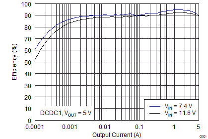
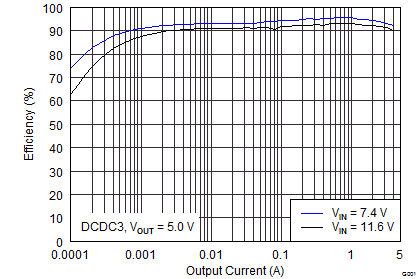
| Efficiency | vs Output Current, DCDC1, VOUT = 5 V | Figure 2 |
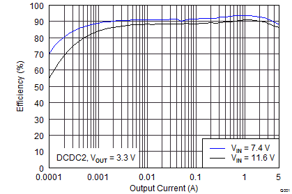
| vs Output Current, DCDC2, VOUT = 3.3 V | Figure 3 | |
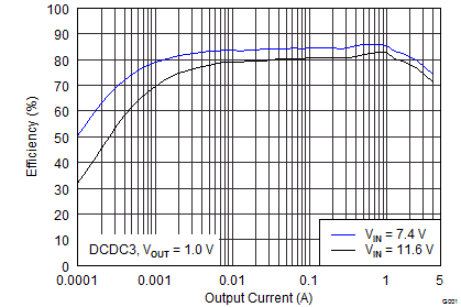
| vs Output Current, DCDC3, VOUT = 1 V | Figure 4 | |
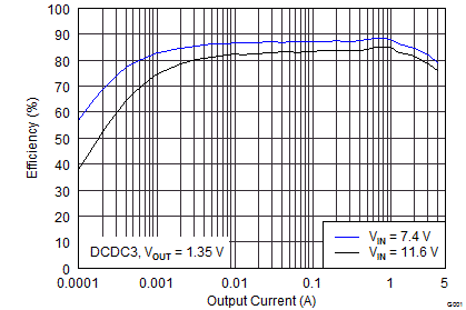
| vs Output Current, DCDC3, VOUT = 1.35 V | Figure 5 | |
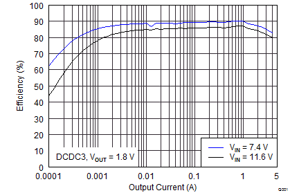
| vs Output Current, DCDC3, VOUT = 1.8 V | Figure 6 | |
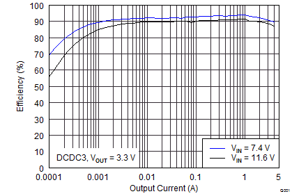
| vs Output Current, DCDC3, VOUT = 3.3 V | Figure 7 | |
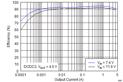
| vs Output Current, DCDC3, VOUT = 4 V | Figure 8 | |
| vs Output Current, DCDC3, VOUT = 5 V | Figure 9 | |
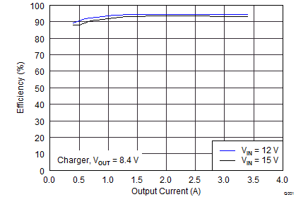
| Efficiency | vs Output Current, Charger, VOUT = 8.4 V | Figure 10 |
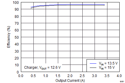
| vs Output Current, Charger, VOUT = 12.6 V | Figure 11 | |
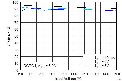
| Efficiency | vs Input Voltage, DCDC1, VOUT = 5 V | Figure 12 |
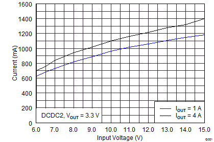
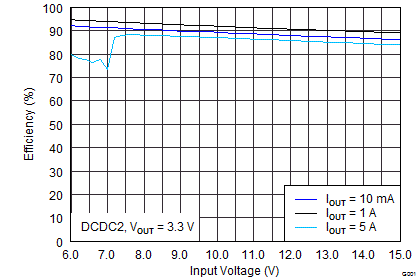
| vs Input Voltage, DCDC2, VOUT = 3.3 V | Figure 13 | |
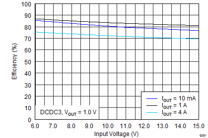
| vs Input Voltage, DCDC3, VOUT = 1 V | Figure 14 | |
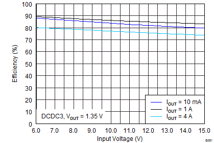
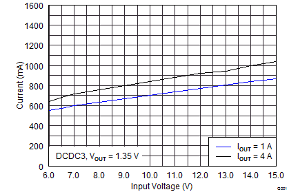
| vs Input Voltage, DCDC3, VOUT = 1.35 V | Figure 15 | |
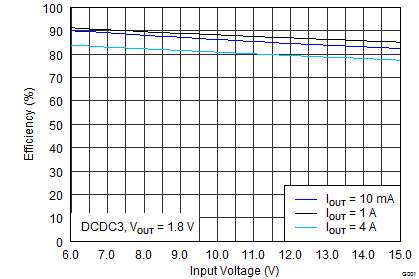
| vs Input Voltage, DCDC3, VOUT = 1.8 V | Figure 16 | |
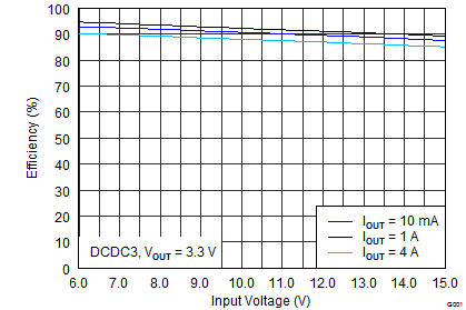
| vs Input Voltage, DCDC3, VOUT = 3.3 V | Figure 17 | |
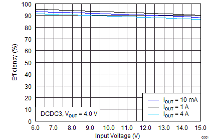
| vs Input Voltage, DCDC3, VOUT = 4 V | Figure 18 | |
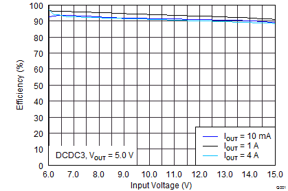
| vs Input Voltage, DCDC3, VOUT = 5 V | Figure 19 | |
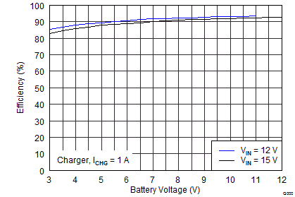
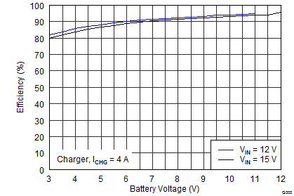
| Efficiency | vs Battery Voltage, Charger, IOUT = 1 A | Figure 20 |
| vs Battery Voltage, Charger, IOUT = 2 A | Figure 21 | |
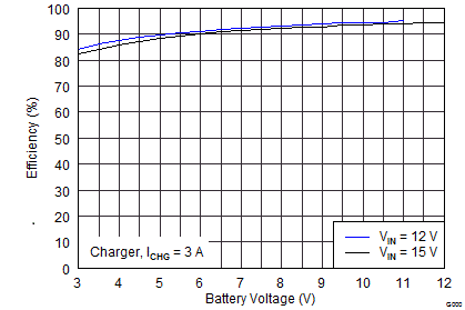
| vs Battery Voltage, Charger, IOUT = 3 A | Figure 22 | |
| vs Battery Voltage, Charger, IOUT = 4 A | Figure 23 | |
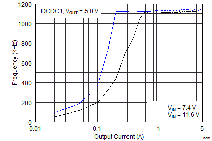
| Switching frequency | vs Output Current, DCDC1, VOUT = 5 V | Figure 24 |
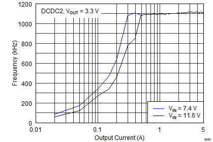
| vs Output Current, DCDC2, VOUT = 3.3 V | Figure 25 | |
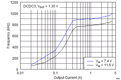
| vs Output Current, DCDC3, VOUT = 1.35 V | Figure 26 | |
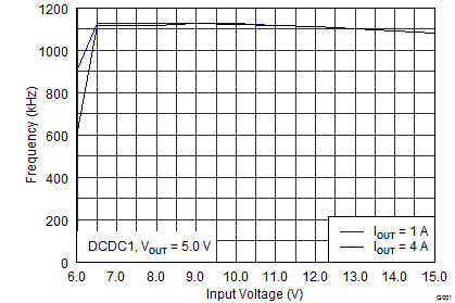
| vs Input Voltage, DCDC1, VOUT = 5 V | Figure 27 | |
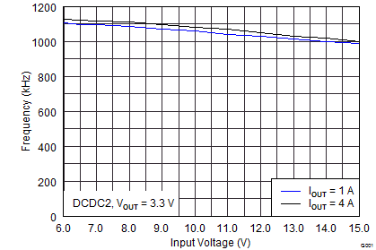
| vs Input Voltage, DCDC2, VOUT = 3.3 V | Figure 28 | |
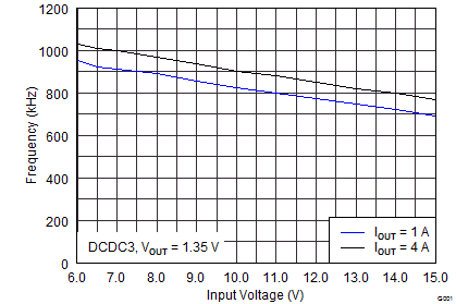
| vs Input Voltage, DCDC3, VOUT = 1.35 V | Figure 29 | |
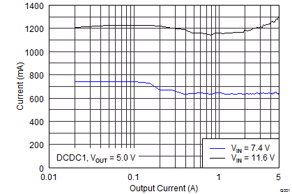
| Inductor current ripple | vs Output Current, DCDC1, VOUT = 5 V | Figure 30 |
| vs Output Current, DCDC2, VOUT = 3.3 V | Figure 31 | |
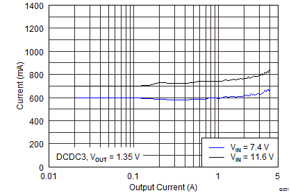
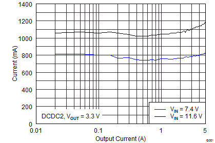
| vs Output Current, DCDC3, VOUT = 1.35 V | Figure 32 | |
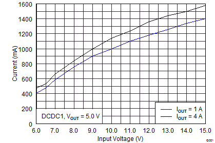
| vs Input Voltage, DCDC1, VOUT = 5 V | Figure 33 | |
| vs Input Voltage, DCDC2, VOUT = 3.3 V | Figure 34 | |
| vs Input Voltage, DCDC3, VOUT = 1.35 V | Figure 35 | |
