SLVS493E March 2004 – April 2022 TPS65130 , TPS65131
PRODUCTION DATA
- 1 Features
- 2 Applications
- 3 Description
- 4 Revision History
- 5 Pin Configuration and Functions
- 6 Specifications
- 7 Detailed Description
-
8 Applications and Implementation
- 8.1 Application Information
- 8.2
Typical Application
- 8.2.1 Design Requirements
- 8.2.2 Detailed Design Procedure
- 8.2.3 Analog Supply Filter
- 8.2.4 Application Curves
- 9 Layout
- 10Device and Documentation Support
- 11Mechanical, Packaging, and Orderable Information
Package Options
Refer to the PDF data sheet for device specific package drawings
Mechanical Data (Package|Pins)
- RGE|24
Thermal pad, mechanical data (Package|Pins)
- RGE|24
Orderable Information
8.2.2.3.2 Output Capacitors
One of the major parameters necessary to define the capacitance value of the output capacitor is the maximum allowed output voltage ripple of the converter. This ripple is determined by two parameters of the capacitor, the capacitance and the ESR. It is possible to calculate the minimum capacitance needed for the defined ripple, supposing that the ESR is zero. Use Equation 7 for the boost converter output capacitor (C4min) and Equation 8 for the inverting converter output capacitor (C5min).
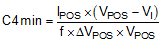
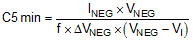
The parameter f is the switching frequency. ΔVPOS and ΔVNEG are the maximum allowed ripple voltages for each converter. Choosing a ripple voltage in the range of 10 mV requires a minimum capacitance of 12 μF. The total ripple is larger due to the ESR of the output capacitor. Use Equation 9 for he boost converter and Equation 10 for the inverting converter to calculate this additional ripple component.
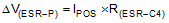
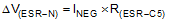
In this example, an additional ripple of 2 mV is the result of using a typical ceramic capacitor with an ESR in the 10-mΩ range. The total ripple is the sum of the ripple caused by the capacitance and the ripple caused by the ESR of the capacitor. In this example, the total ripple is 10 mV.
Load transients can create additional ripple. When the load current increases rapidly, the output capacitor must provide the additional current until the inductor current increases by the control loop which sets a higher ON-time (duty cycle) of the main switch. The higher duty cycle results in longer inductor charging periods. The inductance itself also limits the rate of increase of the inductor current. When the load current decreases rapidly, the output capacitor must store the excess energy (stored in the inductor) until the regulator has decreased the inductor current by reducing the duty cycle. TI recommends using greater capacitance values, as the foregoing calculations show.