SLVS576B SEPTEMBER 2005 – January 2016 TPS65150
PRODUCTION DATA.
- 1 Features
- 2 Applications
- 3 Description
- 4 Revision History
- 5 Pin Configuration and Functions
- 6 Specifications
- 7 Detailed Description
-
8 Application and Implementation
- 8.1 Application Information
- 8.2
Typical Application
- 8.2.1 Design Requirements
- 8.2.2
Detailed Design Procedure
- 8.2.2.1 Boost Converter Design Procedure
- 8.2.2.2 Rectifier Diode Selection
- 8.2.2.3 Setting the Output Voltage
- 8.2.2.4 Output Capacitor Selection
- 8.2.2.5 Input Capacitor Selection
- 8.2.2.6 Compensation
- 8.2.2.7 Negative Charge Pump
- 8.2.2.8 Positive Charge Pump
- 8.2.2.9 Gate Voltage Shaping
- 8.2.2.10 Power-On Sequencing
- 8.2.2.11 Fault Delay
- 8.2.2.12 Undervoltage Lockout Function
- 8.2.3 Application Curves
- 8.3 System Examples
- 9 Power Supply Recommendations
- 10Layout
- 11Device and Documentation Support
- 12Mechanical, Packaging, and Orderable Information
Package Options
Refer to the PDF data sheet for device specific package drawings
Mechanical Data (Package|Pins)
- RGE|24
- PWP|24
Thermal pad, mechanical data (Package|Pins)
Orderable Information
10 Layout
10.1 Layout Guidelines
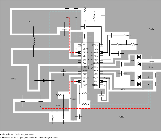
The PCB layout is an important step in the power supply design. An incorrect layout could cause converter instability, load regulation problems, noise, and EMI issues. Especially with a switching DC-DC converter at high load currents, too-thin PCB traces can cause significant voltage spikes. Good grounding is also important. If possible, TI recommends using a common ground plane to minimize ground shifts between analog ground (GND) and power ground (PGND). Additionally, the following PCB design layout guidelines are recommended for the TPS65150 device:
- Boost converter output capacitor, input capacitor and Power ground (PGND) should form a star ground or should be directly connected together on a common power ground plane.
- Place the input capacitor directly from the input pin (VIN) to ground.
- Use a bold PCB trace to connect SUP to the output Vs.
- Place a small bypass capacitor from the SUP pin to ground.
- Use short traces for the charge-pump drive pins (DRVN, DRVP) of VGH and VGL because these traces carry switching currents.
- Place the charge pump flying capacitors as close as possible to the DRVP and DRVN pin, avoiding a high voltage spikes at these pins.
- Place the Schottky diodes as close as possible to the device and to the flying capacitors connected to DRVP and DRVN.
- Carefully route the charge pump traces to avoid interference with other circuits because they carry high voltage switching currents .
- Place the output capacitor of the VCOM buffer as close as possible to the output pin (VCOM).
- The thermal pad must be soldered to the PCB for correct thermal performance.
