SLVS576B SEPTEMBER 2005 – January 2016 TPS65150
PRODUCTION DATA.
- 1 Features
- 2 Applications
- 3 Description
- 4 Revision History
- 5 Pin Configuration and Functions
- 6 Specifications
- 7 Detailed Description
-
8 Application and Implementation
- 8.1 Application Information
- 8.2
Typical Application
- 8.2.1 Design Requirements
- 8.2.2
Detailed Design Procedure
- 8.2.2.1 Boost Converter Design Procedure
- 8.2.2.2 Rectifier Diode Selection
- 8.2.2.3 Setting the Output Voltage
- 8.2.2.4 Output Capacitor Selection
- 8.2.2.5 Input Capacitor Selection
- 8.2.2.6 Compensation
- 8.2.2.7 Negative Charge Pump
- 8.2.2.8 Positive Charge Pump
- 8.2.2.9 Gate Voltage Shaping
- 8.2.2.10 Power-On Sequencing
- 8.2.2.11 Fault Delay
- 8.2.2.12 Undervoltage Lockout Function
- 8.2.3 Application Curves
- 8.3 System Examples
- 9 Power Supply Recommendations
- 10Layout
- 11Device and Documentation Support
- 12Mechanical, Packaging, and Orderable Information
Package Options
Refer to the PDF data sheet for device specific package drawings
Mechanical Data (Package|Pins)
- RGE|24
- PWP|24
Thermal pad, mechanical data (Package|Pins)
Orderable Information
5 Pin Configuration and Functions
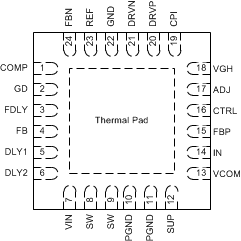
RGE Package
24-Pin VQFN
Top View

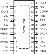
PWP Package
24-Pin HTSSOP
Top View

Pin Functions
| PIN | I/O | DESCRIPTION | ||
|---|---|---|---|---|
| NAME | VQFN | HTSSOP | ||
| ADJ | 17 | 14 | I/O | Gate voltage shaping circuit. Connecting a capacitor to this pin sets the fall time of the positive gate voltage V(VGH). |
| COMP | 1 | 22 | O | This is the compensation pin for the main boost converter. A small capacitor and if required a series resistor is connected to this pin. |
| CPI | 19 | 16 | I | Input of the VGH isolation switch and gate voltage shaping circuit. |
| CTRL | 16 | 13 | I | Control signal for the gate voltage shaping signal. Apply the control signal for the gate voltage control. Usually the timing controller of the LCD panel generates this signal. If this function is not required, this pin must be connected to VI. By doing this, the internal switch between CPI and VGH provides isolation for the positive charge pump output V(VGH). DLY2 sets the delay time for V(VGH) to come up. |
| DLY1 | 5 | 2 | I/O | Power-on sequencing adjust. Connecting a capacitor from this pin to ground allows to set the delay time between the boost converter output V(VS) and the negative charge pump V(VGL) during start-up. |
| DLY2 | 6 | 3 | I/O | Power-on sequencing adjust. Connecting a capacitor from this pin to ground allows to set the delay time between the negative charge pump V(VGL) and the positive charge pump during start-up. Note that Q5 in the gate voltage shaping block only turns on when the positive charge pump is within regulation. (This provides input-output isolation of V(VGH)). |
| DRVN | 21 | 18 | I/O | Negative charge pump driver. |
| DRVP | 20 | 17 | I/O | Positive charge pump driver. |
| FB | 4 | 1 | I | Boost converter feedback sense input. |
| FBN | 24 | 21 | I | Negative charge pump feedback sense input. |
| FBP | 15 | 12 | I | Positive charge pump feedback sense input. |
| FDLY | 3 | 24 | I/O | Fault delay. Connecting a capacitor from this pin to VI sets the delay time from the point when one or more of the of the outputs V(VS), V(VGH), V(VGL) drops below its power good threshold until the device shuts down. To restart the device, the input voltage must be cycled to ground. This feature can be disabled by connecting the FDLY pin to VI. |
| GD | 2 | 23 | I | Active-low, open-drain output. This output is latched low when the boost converter output is in regulation. This signal can be used to drive an external MOSFET to provide isolation for V(VS). |
| GND | 22 | 19 | Analog ground. | |
| IN | 14 | 11 | I | Input of the VCOM buffer. If this pin is connected to ground, the VCOM buffer is disabled. |
| PGND | 10, 11 | 7, 8 | Power ground. | |
| REF | 23 | 20 | O | Internal reference output, typically 1.213 V. |
| SUP | 12 | 9 | I/O | Supply pin of the positive, negative charge pump and boost converter gate drive circuit. This pin should be connected to the output of the main boost converter. |
| SW | 8, 9 | 5, 6 | I | Switch pin of the boost converter. |
| VCOM | 13 | 10 | O | VCOM buffer output. Typically a 1-µF output capacitor is required on this pin. |
| VGH | 18 | 15 | O | Positive output voltage to drive the TFT gates with an adjustable fall time. This pin is internally connected with a MOSFET switch to the positive charge pump input CPI. |
| VIN | 7 | 4 | I | This is the input voltage pin of the device. |
| Thermal Pad | — | — | The thermal pad must to be soldered to GND | |