SLDS206E November 2014 – February 2021 TPS65218
PRODUCTION DATA
- 1 Features
- 2 Applications
- 3 Description
- 4 Revision History
- 5 Pin Configuration and Functions
- 6 Specifications
-
7 Detailed Description
- 7.1 Overview
- 7.2 Functional Block Diagram
- 7.3
Feature Description
- 7.3.1
Wake-Up and Power-Up and Power-Down Sequencing
- 7.3.1.1 Power-Up Sequencing
- 7.3.1.2 Power-Down Sequencing
- 7.3.1.3 Strobe 1 and Strobe 2
- 7.3.1.4 Supply Voltage Supervisor and Power-Good (PGOOD)
- 7.3.1.5 Backup Supply Power-Good (PGOOD_BU)
- 7.3.1.6 Internal LDO (INT_LDO)
- 7.3.1.7 Current Limited Load Switches
- 7.3.1.8 LDO1
- 7.3.1.9 Coin Cell Battery Voltage Acquisition
- 7.3.1.10 UVLO
- 7.3.1.11 Power-Fail Comparator
- 7.3.1.12 Battery-Backup Supply Power-Path
- 7.3.1.13 DCDC3 and DCDC4 Power-Up Default Selection
- 7.3.1.14 I/O Configuration
- 7.3.1.15 Push Button Input (PB)
- 7.3.1.16 AC_DET Input (AC_DET)
- 7.3.1.17 Interrupt Pin (INT)
- 7.3.1.18 I2C Bus Operation
- 7.3.1
Wake-Up and Power-Up and Power-Down Sequencing
- 7.4 Device Functional Modes
- 7.5 Register Maps
- 8 Application and Implementation
- 9 Power Supply Recommendations
- 10Layout
- 11Device and Documentation Support
- 12Mechanical, Packaging, and Orderable Information
Package Options
Mechanical Data (Package|Pins)
Thermal pad, mechanical data (Package|Pins)
Orderable Information
8.2.1.2 Inductor Selection for Buck Converters
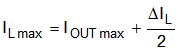
The inductor value affects its peak to peak ripple current, the PWM to PFM transition point, the output voltage ripple, and the efficiency. The selected inductor must be rated for its DC resistance and saturation current. The inductor ripple current (∆L) decreases with higher inductance and increases with higher VIN or VOUT. Equation 1 calculates the maximum inductor current ripple under static load conditions. The saturation current of the inductor should be rated higher than the maximum inductor current as calculated with Equation 2. This is recommended as during heavy load transient the inductor current will rise above the calculated value.
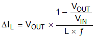
where
- F = Switching frequency
- L = Inductor value
- ∆IL = Peak-to-peak inductor ripple current
- ILmax = Maximum inductor current
The following inductors have been used with the TPS65218 (see Table 8-1).
| PART NUMBER | VALUE | SIZE (mm) [L × W × H] | MANUFACTURER |
|---|---|---|---|
| INDUCTORS FOR DCDC1, DCDC2, DCDC3, DCDC4 | |||
| SPM3012T-1R5M | 1.5 µH, 2.8 A, 77 mΩ | 3.2 × 3.0 × 1.2 | TDK |
| IHLP1212BZER1R5M11 | 1.5 µH, 4.0 A, 28.5 mΩ | 3.6 × 3.0 × 2.0 | Vishay |
| INDUCTORS FOR DCDC5, DCDC6 | |||
| MLZ2012N100L | 10 µH, 110 mA, 300 mΩ | 2012 / 0805 (2.00 × 1.25 × 1.25) | TDK |
| LQM21FN100M80 | 10 µH, 100 mA, 300 mΩ | 2012 / 0805 (2.00 × 1.25 × 1.25) | Murata |