SLDS261A November 2019 – February 2021 TPS6521815
PRODUCTION DATA
- 1 Features
- 2 Applications
- 3 Description
- 4 Revision History
- 5 Description (continued)
- 6 Pin Configuration and Functions
- 7 Specifications
-
8 Detailed Description
- 8.1 Overview
- 8.2 Functional Block Diagram
- 8.3
Feature Description
- 8.3.1
Wake-Up and Power-Up and Power-Down Sequencing
- 8.3.1.1 Power-Up Sequencing
- 8.3.1.2 Power-Down Sequencing
- 8.3.1.3 Strobe 1 and Strobe 2
- 8.3.1.4 Supply Voltage Supervisor and Power-Good (PGOOD)
- 8.3.1.5 Backup Supply Power-Good (PGOOD_BU)
- 8.3.1.6 Internal LDO (INT_LDO)
- 8.3.1.7 Current Limited Load Switches
- 8.3.1.8 LDO1
- 8.3.1.9 Coin Cell Battery Voltage Acquisition
- 8.3.1.10 UVLO
- 8.3.1.11 Power-Fail Comparator
- 8.3.1.12 Battery-Backup Supply Power-Path
- 8.3.1.13 DCDC3 and DCDC4 Power-Up Default Selection
- 8.3.1.14 I/O Configuration
- 8.3.1.15 Push Button Input (PB)
- 8.3.1.16 AC_DET Input (AC_DET)
- 8.3.1.17 Interrupt Pin (INT)
- 8.3.1.18 I2C Bus Operation
- 8.3.1
Wake-Up and Power-Up and Power-Down Sequencing
- 8.4 Device Functional Modes
- 8.5 Programming
- 8.6 Register Maps
- 9 Application and Implementation
- 10Power Supply Recommendations
- 11Layout
- 12Device and Documentation Support
- 13Mechanical, Packaging, and Orderable Information
Package Options
Mechanical Data (Package|Pins)
- RSL|48
Thermal pad, mechanical data (Package|Pins)
- RSL|48
Orderable Information
8.3.1.5 Backup Supply Power-Good (PGOOD_BU)
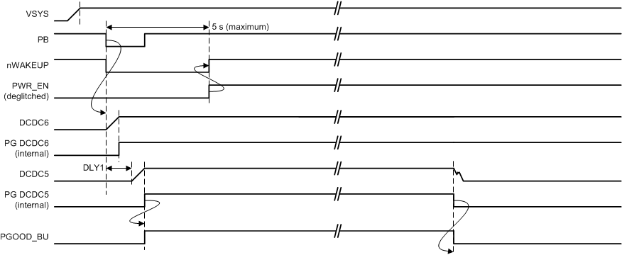
PGOOD_BU is a push-pull output indicating if DCDC5 and DCDC6 are in regulation. The output is driven to high when both rails are in regulation, and driven low if at least one of the rails is below the power-good threshold. The output-high level is equal to the output voltage of DCDC6.
PGOOD_BU is the logical and between PGOOD (DCDC5) and PGOOD (DCDC6), and has no delay time built-in. Unlike the main power-good, a fault on DCDC5 or DCDC6 does not trigger the power-down sequencer, does not disable any of the rails in the system, and has no effect on the PGOOD pin. DCDC5 and DCDC6 recover automatically once the fault is removed.
In this example, the power-down is triggered by a fault on DCDC3.
This timing diagram assumes each rail powers up within the strobe delay time. If a rail takes longer than the strobe delay time to power up, the next rail will wait for the previous rail to reach its PGOOD voltage, and then may wait an additional 1 ms until it is enabled.
