SLVSCN5B june 2014 – may 2023 TPS65262-1
PRODUCTION DATA
- 1
- 1 Features
- 2 Applications
- 3 Description
- 4 Revision History
- 5 Device Comparison Table
- 6 Pin Configuration and Functions
- 7 Specifications
-
8 Detailed Description
- 8.1 Overview
- 8.2 Functional Block Diagram
- 8.3
Feature Description
- 8.3.1 Adjusting the Output Voltage
- 8.3.2 Enable and Adjusting UVLO
- 8.3.3 Soft-Start Time
- 8.3.4 Power-Up Sequencing
- 8.3.5 V7V Low Dropout Regulator and Bootstrap
- 8.3.6 Out-of-Phase Operation
- 8.3.7 Output Overvoltage Protection (OVP)
- 8.3.8 PSM
- 8.3.9 Slope Compensation
- 8.3.10 Overcurrent Protection (OCP)
- 8.3.11 Power Good
- 8.3.12 Thermal Shutdown
- 8.4 Device Functional Modes
- 9 Application and Implementation
- 10Device and Documentation Support
- 11Mechanical, Packaging, and Orderable Information
Package Options
Mechanical Data (Package|Pins)
- RHB|32
Thermal pad, mechanical data (Package|Pins)
- RHB|32
Orderable Information
8.3.1 Adjusting the Output Voltage
The output voltage of each buck is set with a resistor divider from the output of buck to the FB pin. TI recommends to use 1% tolerance, or better, divider resistors.
 Figure 8-1 Voltage Divider Circuit
Equation 1. 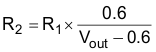
To improve efficiency at light loads, consider using larger value resistors. If the values are too high, the regulator is more sensitive to noise. Table 8-1 shows the recommended resistor values.
Table 8-1 Output Resistor Divider Selection
| Output Voltage (V) | R1 (kΩ) | R2 (kΩ) |
|---|---|---|
| 1 | 10 | 15 |
| 1.2 | 10 | 10 |
| 1.5 | 15 | 10 |
| 1.8 | 20 | 10 |
| 2.5 | 31.6 | 10 |
| 3.3 | 45.3 | 10 |
| 3.3 | 22.6 | 4.99 |
| 5 | 73.2 | 10 |
| 5 | 36.5 | 4.99 |