SLVSCN5B june 2014 – may 2023 TPS65262-1
PRODUCTION DATA
- 1
- 1 Features
- 2 Applications
- 3 Description
- 4 Revision History
- 5 Device Comparison Table
- 6 Pin Configuration and Functions
- 7 Specifications
-
8 Detailed Description
- 8.1 Overview
- 8.2 Functional Block Diagram
- 8.3
Feature Description
- 8.3.1 Adjusting the Output Voltage
- 8.3.2 Enable and Adjusting UVLO
- 8.3.3 Soft-Start Time
- 8.3.4 Power-Up Sequencing
- 8.3.5 V7V Low Dropout Regulator and Bootstrap
- 8.3.6 Out-of-Phase Operation
- 8.3.7 Output Overvoltage Protection (OVP)
- 8.3.8 PSM
- 8.3.9 Slope Compensation
- 8.3.10 Overcurrent Protection (OCP)
- 8.3.11 Power Good
- 8.3.12 Thermal Shutdown
- 8.4 Device Functional Modes
- 9 Application and Implementation
- 10Device and Documentation Support
- 11Mechanical, Packaging, and Orderable Information
Package Options
Mechanical Data (Package|Pins)
- RHB|32
Thermal pad, mechanical data (Package|Pins)
- RHB|32
Orderable Information
9.2.2.1 Output Inductor Selection
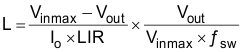
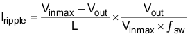
To calculate the value of the output inductor, use Equation 6. LIR is a coefficient that represents the amount of inductor ripple current relative to the maximum output current. The inductor ripple current is filtered by the output capacitor. Therefore, choosing high inductor ripple currents impact the selection of the output capacitor because the output capacitor must have a ripple current rating equal to or greater than the inductor ripple current. In general, the inductor ripple value is at the discretion of the designer; however, LIR is normally from 0.1 to 0.3 for the majority of applications.
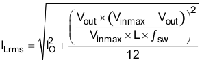
For the output filter inductor, it is important not to exceed the RMS current and saturation current ratings. The RMS and peak inductor current can be found from Equation 8 and Equation 9.
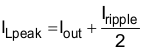
The current flowing through the inductor is the inductor ripple current plus the output current. During power-up, faults, or transient load conditions, the inductor current can increase above the calculated peak inductor current level calculated previously. In transient conditions, the inductor current can increase up to the switch current limit of the device. For this reason, the most conservative approach is to specify an inductor with a saturation current rating equal to or greater than the switch current limit rather than the peak inductor current.