SLVSCQ2 July 2015 TPS65400-Q1
PRODUCTION DATA.
- 1 Features
- 2 Applications
- 3 Description
- 4 Revision History
- 5 Description (continued)
- 6 Pin Configuration and Functions
- 7 Specifications
-
8 Detailed Description
- 8.1 Overview
- 8.2 Functional Block Diagrams
- 8.3
Feature Description
- 8.3.1 Startup Timing and Power Sequencing
- 8.3.2 UVLO and Precision Enables
- 8.3.3 Soft-Start and Prebiased Startup
- 8.3.4 PWM Switching Frequency Selection
- 8.3.5 Clock Synchronization
- 8.3.6 Phase Interleaving
- 8.3.7 Fault Handling
- 8.3.8 OCP for SW1 to SW4
- 8.3.9 Overcurrent Protection for SW1 to SW4 in Current Sharing Operation
- 8.3.10 Recovery on Power Loss
- 8.3.11 Feedback Compensation
- 8.3.12 Adjusting Output Voltage
- 8.3.13 Digital Interface - PMBus
- 8.3.14 Initial Configuration
- 8.4 Device Functional Modes
- 8.5
Register Maps
- 8.5.1 PMBus
- 8.5.2 PMBus Register Descriptions
- 8.5.3
PMBus Core Commands
- 8.5.3.1 (00h) PAGE
- 8.5.3.2 (01h) OPERATION
- 8.5.3.3 (03h) CLEAR_FAULTS
- 8.5.3.4 (10h) WRITE_PROTECT
- 8.5.3.5 (11h) STORE_DEFAULT_ALL
- 8.5.3.6 (19h) CAPABILITY
- 8.5.3.7 (78h) STATUS_BYTE
- 8.5.3.8 (79h) STATUS_WORD
- 8.5.3.9 (7Ah) STATUS_VOUT
- 8.5.3.10 (80h) STATUS_MFR_SPECIFIC
- 8.5.3.11 (98h) PMBUS_REVISION
- 8.5.3.12 (ADh) IC_DEVICE_ID
- 8.5.3.13 (AEh) IC_DEVICE_REV
- 8.5.4
Manufacturer-Specific Commands
- 8.5.4.1 (D0h) USER_DATA_BYTE_00
- 8.5.4.2 (D1h) USER_DATA_BYTE_01
- 8.5.4.3 (D2h) PIN_CONFIG_00
- 8.5.4.4 (D3h) PIN_CONFIG_01
- 8.5.4.5 (D4h) SEQUENCE_CONFIG
- 8.5.4.6 (D5h) SEQUENCE_ORDER
- 8.5.4.7 (D6h) IOUT_MODE
- 8.5.4.8 (D7h) FREQUENCY_PHASE
- 8.5.4.9 (D8h) VREF_COMMAND
- 8.5.4.10 (D9h) IOUT_MAX
- 8.5.4.11 (DAh) USER_RAM_00
- 8.5.4.12 (DBh) SOFT_RESET
- 8.5.4.13 (DCh) RESET_DELAY
- 8.5.4.14 (DDh) TON_TOFF_DELAY
- 8.5.4.15 (DEh) TON_TRANSITION_RATE
- 8.5.4.16 (DFh) VREF_TRANSITION_RATE
- 8.5.4.17 (F0h) SLOPE_COMPENSATION
- 8.5.4.18 (F1h) ISENSE_GAIN
- 8.5.4.19 (FCh) DEVICE_CODE
- 9 Application and Implementation
- 10Power Supply Recommendations
- 11Layout
- 12Device and Documentation Support
- 13Mechanical, Packaging, and Orderable Information
Package Options
Mechanical Data (Package|Pins)
- RGZ|48
Thermal pad, mechanical data (Package|Pins)
- RGZ|48
Orderable Information
1 Features
- Qualified for Automotive Applications
- AEC-Q100 Qualified With the Following Results:
- Device Temperature Grade 1: –40°C to 125°C Ambient Operating Temperature Range
- Device HBM ESD Classification Level H2
- Device CDM ESD Classification Level C4B
- Efficiency up to 95% for Each Switching Regulator
- Switching Regulator Specifications:
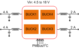
- Input Voltage Range: 4.5 to 18 V
- Vout Range: 0.6 V-90%Vin
- SW1, SW2 Iout: 4-A Max
- SW3, SW4 Iout: 2-A Max
- Pre-Bias Startup Algorithm Minimizes Voltage Dip During Startup
- Internal Undervoltage Lockout (UVLO), Overcurrent Protection (OCP), Overvoltage Protection (OVP), and Overtemperature Protection (OTP)
- Thermally-Enhanced 7-mm × 7-mm 48-Pin, 0.5-mm Pitch VQFN Package
- Pin Accessible Features:
- Adjustable VOUT With External Feedback Resistors
- Sequencing Control Through Precision Enable Pins for Each Switcher
- Resistor Adjustable PWM Switching Frequency from 275 kHz to 2.2 MHz
- Clock Sync Input and Clock Output
- Soft-Start Delay Through External Capacitor
- Current Sharing Between SW1 and SW2 and Between SW3 and SW4 Allows Support of Higher Current Needs if Required
- PMBus Runtime Control and Status
- Runtime Voltage Positioning Through Adjustment of VREF
- Enable and Disable of Each Switcher
- Fault and Status Monitoring
- User-Configurable PMBus / I2C Options, Saved in EEPROM
- Power Supply Turn-On and Turn-Off Sequencing
- Sequencing can be Based on Fixed Time Delays or PGOOD Dependence
- Initial Voltage Positioning Through VREF Configuration
- PWM Frequency Adjustment for Each Switcher
- Individual PWM Phase Alignment for Each Switcher to Minimize Ripple and Capacitor Size
- Adjustable Current Limit on Each Regulator Enables Size and Cost Optimization of Inductors
- Soft-Start Time
2 Applications
- Qualified for Automotive Applications
- Small Cellular Base Stations (BTS) (for Example: Picocells and Microcells); Macro BTS (Using Multiple PMUs)
- Power over Ethernet (PoE) Powered Communications Infrastructure Equipment
- Powering DSP and MCUs
- Industrial and Factory Automation
- Systems Requiring Small Form Factor, High-Efficiency, High-Ambient Operating Temperature, and Flexible Power Management
3 Description
The TPS65400-Q1 is an integrated PMU optimized for applications requiring small form factor and high power conversion efficiency, enabling small space-constrained equipment with high ambient operating temperature without cooling. It provides high-power efficiency at a system level by enabling a single stage conversion from an intermediate distribution bus with an optimized combination of regulators.
Device Information(1)
| PART NUMBER | PACKAGE | BODY SIZE (NOM) |
|---|---|---|
| TPS65400-Q1 | VQFN (48) | 7.00 mm × 7.00 mm |
- For all available packages, see the orderable addendum at the end of the data sheet.
Simplified Schematic

4 Revision History
| DATE | REVISION | NOTES |
|---|---|---|
| July 2015 | * | Initial release. |