SLVSCQ2 July 2015 TPS65400-Q1
PRODUCTION DATA.
- 1 Features
- 2 Applications
- 3 Description
- 4 Revision History
- 5 Description (continued)
- 6 Pin Configuration and Functions
- 7 Specifications
-
8 Detailed Description
- 8.1 Overview
- 8.2 Functional Block Diagrams
- 8.3
Feature Description
- 8.3.1 Startup Timing and Power Sequencing
- 8.3.2 UVLO and Precision Enables
- 8.3.3 Soft-Start and Prebiased Startup
- 8.3.4 PWM Switching Frequency Selection
- 8.3.5 Clock Synchronization
- 8.3.6 Phase Interleaving
- 8.3.7 Fault Handling
- 8.3.8 OCP for SW1 to SW4
- 8.3.9 Overcurrent Protection for SW1 to SW4 in Current Sharing Operation
- 8.3.10 Recovery on Power Loss
- 8.3.11 Feedback Compensation
- 8.3.12 Adjusting Output Voltage
- 8.3.13 Digital Interface - PMBus
- 8.3.14 Initial Configuration
- 8.4 Device Functional Modes
- 8.5
Register Maps
- 8.5.1 PMBus
- 8.5.2 PMBus Register Descriptions
- 8.5.3
PMBus Core Commands
- 8.5.3.1 (00h) PAGE
- 8.5.3.2 (01h) OPERATION
- 8.5.3.3 (03h) CLEAR_FAULTS
- 8.5.3.4 (10h) WRITE_PROTECT
- 8.5.3.5 (11h) STORE_DEFAULT_ALL
- 8.5.3.6 (19h) CAPABILITY
- 8.5.3.7 (78h) STATUS_BYTE
- 8.5.3.8 (79h) STATUS_WORD
- 8.5.3.9 (7Ah) STATUS_VOUT
- 8.5.3.10 (80h) STATUS_MFR_SPECIFIC
- 8.5.3.11 (98h) PMBUS_REVISION
- 8.5.3.12 (ADh) IC_DEVICE_ID
- 8.5.3.13 (AEh) IC_DEVICE_REV
- 8.5.4
Manufacturer-Specific Commands
- 8.5.4.1 (D0h) USER_DATA_BYTE_00
- 8.5.4.2 (D1h) USER_DATA_BYTE_01
- 8.5.4.3 (D2h) PIN_CONFIG_00
- 8.5.4.4 (D3h) PIN_CONFIG_01
- 8.5.4.5 (D4h) SEQUENCE_CONFIG
- 8.5.4.6 (D5h) SEQUENCE_ORDER
- 8.5.4.7 (D6h) IOUT_MODE
- 8.5.4.8 (D7h) FREQUENCY_PHASE
- 8.5.4.9 (D8h) VREF_COMMAND
- 8.5.4.10 (D9h) IOUT_MAX
- 8.5.4.11 (DAh) USER_RAM_00
- 8.5.4.12 (DBh) SOFT_RESET
- 8.5.4.13 (DCh) RESET_DELAY
- 8.5.4.14 (DDh) TON_TOFF_DELAY
- 8.5.4.15 (DEh) TON_TRANSITION_RATE
- 8.5.4.16 (DFh) VREF_TRANSITION_RATE
- 8.5.4.17 (F0h) SLOPE_COMPENSATION
- 8.5.4.18 (F1h) ISENSE_GAIN
- 8.5.4.19 (FCh) DEVICE_CODE
- 9 Application and Implementation
- 10Power Supply Recommendations
- 11Layout
- 12Device and Documentation Support
- 13Mechanical, Packaging, and Orderable Information
Package Options
Mechanical Data (Package|Pins)
- RGZ|48
Thermal pad, mechanical data (Package|Pins)
- RGZ|48
Orderable Information
9 Application and Implementation
NOTE
Information in the following applications sections is not part of the TI component specification, and TI does not warrant its accuracy or completeness. TI’s customers are responsible for determining suitability of components for their purposes. Customers should validate and test their design implementation to confirm system functionality.
9.1 Application Information
The TPS65400-Q1 PMU is designed to support the trend towards smaller space-constrained systems, which require high-efficiency to limit power dissipation in a closed environment. The TPS65400-Q1 is intended to provide a complete highly-efficiency power management solution in a small form factor while providing maximum control through the I2C bus and ease of use.
The TPS65400-Q1 can support input voltages from 4.5 to 18 V, allowing it to be used in systems powered from a single 5- or 12-V intermediate power bus. High system power conversion efficiency is achieved by providing a single-stage conversion from, for example, the 12-V input voltage to the high-current voltage rails required by the digital circuits.
The two buck regulators SW1 and SW2 can provide an output voltage in the range of 0.6 V to 90%Vin and up to 4-A peak continuous current.
The two buck regulators SW3 and SW4 can provide an output voltage in the range of 0.6 V to 90%Vin and up to 2-A peak continuous current.
9.2 Typical Applications
9.2.1 Internal Operation Typical Application
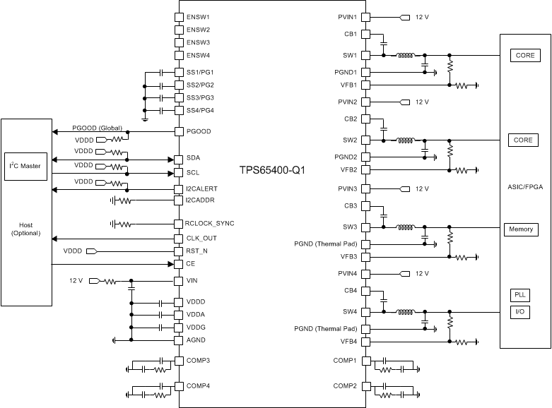 Figure 32. Typical Application Schematic
9.2.1.1 Design Requirements
Table 42 lists PMBus commands to configure this device.
Table 42. PMBus Commands Used for Internal Operation
| COMMAND NAME | CODE | NAME | BITS | COMMENT |
|---|---|---|---|---|
| PAGE | 00h | — | 7:0 | Selects output rail |
| STORE_DEFAULT_ALL | 11h | — | — | Save settings as default |
| PIN_CONFIG_00 | D2h | PGOOD_PIN_CONFIG | 6:2 | Configure PGOOD pin to mask PGOOD4 |
| ENABLE_PIN_CONFIG(1) | 1:0 | Active ENABLE (manufacturer default) | ||
| PIN_CONFIG_01 | D3h | SSPG_PIN_CONFIG | 0 | Set to PG for internal soft-start |
| SEQUENCE_CONFIG | D4h | START_PGOOD | 0 | Disable PGOOD dependence |
| SEQUENCE_ORDER | D5h | START_ORDER | 3:2 | Start sequence order |
| STOP_ORDER | 1:0 | Stop sequence order | ||
| RESET_DELAY | DCh | RESET_DELAY(1) | 2:0 | Reset delay time |
| TON_TOFF_DELAY | DDh | TON_DELAY | 5:3 | Delay time before starting |
| TOFF_DELAY | 2:0 | Delay time before stopping | ||
| TON_TRANSITION_RATE | DEh | TON_RAMP_RATE | 1:0 | Internal soft-start ramping rate |
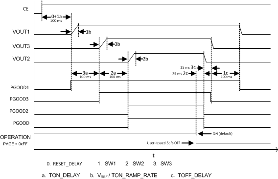
To achieve the timing requirements shown in Table 42, an example configuration script is shown in Table 43.
Table 43. Example Configuration Script for Internal Operation
| COMMAND NAME | CODE | WRITE BYTE | COMMENT |
|---|---|---|---|
| PAGE | 00h | 0xFF | Selects all |
| PIN_CONFIG_00 | D2h | 0x1C | PGOOD pin is a function of PGOOD1 and PGOOD2 and PGOOD3 |
| SEQUENCE_CONFIG | D4h | 0x01 | Disable PGOOD dependence |
| RESET_DELAY(1) | DCh | 0x02 | 100-ms reset delay |
| PAGE | 00h | 0x00 | Selects SW1 |
| PIN_CONFIG_01 | D3h | 0x01 | Configure SS1/PG1 pin to PG1 for internal soft-start |
| SEQUENCE_ORDER | D5h | 0x08 | First to Start, third to Stop |
| TON_TOFF_DELAY | DDh | 0x04 | 0-ms turn-on delay 100-ms turn-off delay |
| TON_TRANSITION_RATE | DEh | TON_RAMP_RATE | Internal soft-start ramping rate |
| PAGE | 00h | 0x02 | Selects SW3 |
| PIN_CONFIG_01 | D3h | 0x01 | Configure SS3/PG3 pin to PG3 for internal soft-start |
| SEQUENCE_ORDER | D5h | 0x05 | Second to start, second to stop |
| TON_TOFF_DELAY | DDh | 0x23 | 100-ms turn-on delay 25-ms turn-off delay |
| TON_TRANSITION_RATE | DEh | TON_RAMP_RATE | Internal soft-start ramping rate |
| PAGE | 00h | 0x01 | Selects SW2 |
| PIN_CONFIG_01 | D3h | 0x01 | Configure SS2/PG2 pin to PG2 for internal soft-start |
| SEQUENCE_ORDER | D5h | 0x02 | Third to start, first to stop |
| TON_TOFF_DELAY | DDh | 0x23 | 100-ms turn-on delay 25-ms turn-off delay |
| TON_TRANSITION_RATE | DEh | TON_RAMP_RATE | Internal soft-start ramping rate |
| STORE_DEFAULT_ALL | 11h | — | Save settings as default |
9.2.1.2 Detailed Design Procedure
9.2.1.2.1 Component Selection
9.2.1.2.1.1 Output Inductor Selection
Equation 9 gives the current ripple flowing in the inductor in CCM.

where
- ΔIL is the current ripple in the inductor.
- Vout is the output voltage.
- Vin is the input voltage of the converter.
- L is the value of the inductor in henry.
- ƒSW is the switching frequency of the converter.
Typically, the value of L is chosen to have the ripple current be 0.1× to 0.3× the full-load current. Choose the inductor so that the saturation current is higher than the maximum expected current plus half the current ripple at maximum operating temperature.
9.2.1.2.1.2 Output Capacitor Selection
The output capacitor needs to be properly sized to reduce voltage ripple due to the switching action (ripple voltage) and to reduce output voltage swings during transient load currents. Equation 10 gives the output voltage ripple.

Equation 11 gives the voltage variation during output current transients.

9.2.1.2.2 Internal Operation With Some Switchers Disabled
For applications where the internal settings for sequencing and soft-start are sufficient, all used output rails should have their enable terminals ENSWx tied high or floating and all unused output rails should have their enable pins ENSWx tied low for the default active ENABLE setting of ENABLE_PIN_CONFIG. This prevents the device from turning on an unused output by software default from an OPERATION ON request. This requirement extends to unpowered switchers; if a pair of switchers is unused, then both ENSWx pins must be tied low.
9.2.1.2.3 Internal Operation With All Switchers Enabled
For applications where all outputs rails will be used, it is sufficient to leave all enable terminals ENSWx disconnected and to set ENABLE_PIN_CONFIG to inactive.
9.2.1.2.4 Example Configuration
Figure 33 shows an internal sequencing schematic example where only switchers 1 to 3 are used for a set of timing requirements. If the internal configuration and fault handling is sufficient, and provided that the user configures the chip through SDA/SCL before placing it on a target board, then it is not necessary for a supervisory and housekeeping host controller chip like a MCU or DSP to be connected to the TPS65400-Q1. In such a case, digital terminals PGOOD, SSx/PG, SDA/SCL, I2CALERT, and CLK_OUT can be left unconnected with no pull-ups required, during normal operation. RST_N can be tied directly to VDDD (no pull-up required). I2CADDR can be tied directly to VDDD after programming. Control line CE can be left unconnected if the chip is constantly powered after VIN is provided.
9.2.1.2.5 Unused Switchers
If the default setting active ENABLE of ENABLE_PIN_CONFIG is selected, ENSWx for unused switchers must always be tied low.
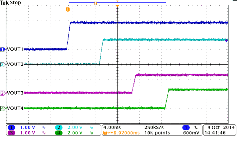
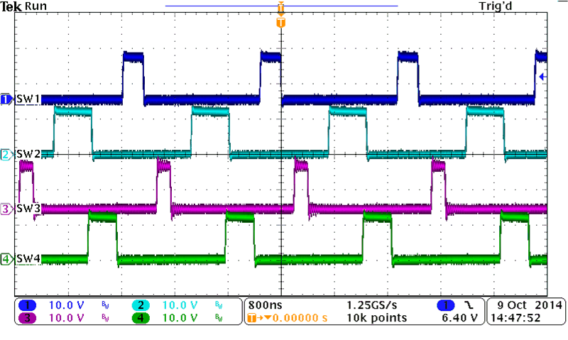
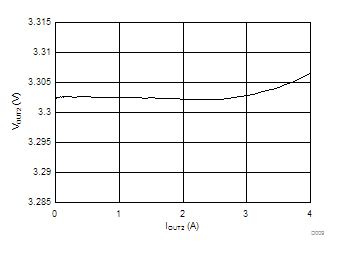
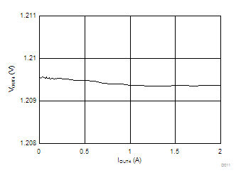
9.2.1.3 Application Curves
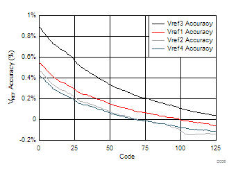
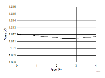
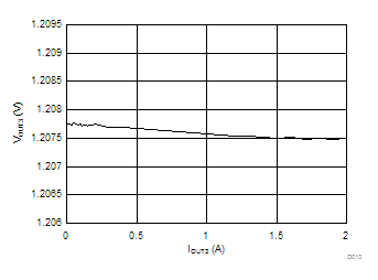
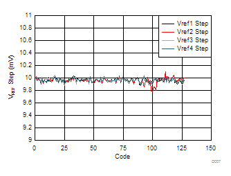
9.2.2 Current Sharing Typical Application
An example configuration is shown where both pairs of outputs are current shared. Soft-start time is configured externally with capacitors (this is the default setting) and ENABLE_PIN_CONFIG is set to single ENABLE.
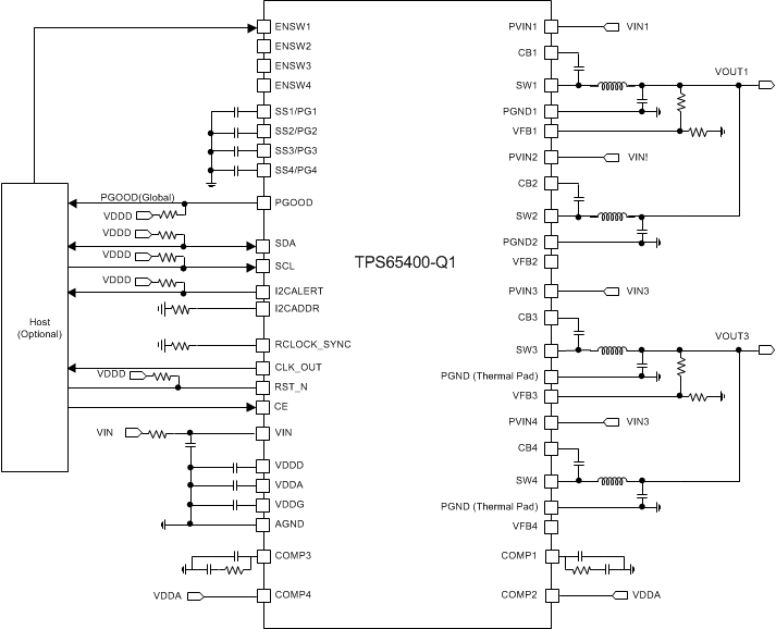 Figure 42. Current Sharing Schematic
9.2.2.1 Design Requirements
Table 44 lists PMBus commands to configure this device.
Table 44. PMBus Commands Used for Current Sharing With Single-Pin Enable(1)
| COMMAND NAME | CODE | NAME | BITS | COMMENT |
|---|---|---|---|---|
| PAGE | 00h | — | 7:0 | Selects output rail |
| STORE_DEFAULT_ALL | 11h | — | — | Save settings as default |
| PIN_CONFIG_00 | D2h | PGOOD_PIN_CONFIG(1) | 6:2 | PGOOD pin and of all PGOOD (manufacturer default) |
| ENABLE_PIN_CONFIG | 1:0 | Single ENABLE | ||
| PIN_CONFIG_01 | D3h | SSPG_PIN_CONFIG(1) | 0 | Set to SSx for external soft-start (manufacturer default) |
| SEQUENCE_CONFIG | D4h | START_PGOOD(1) | 0 | Enable PGOOD dependence (manufacturer default) |
| SEQUENCE_ORDER | D5h | START_ORDER | 3:2 | Start sequence order |
| STOP_ORDER | 1:0 | Stop sequence order | ||
| TON_TOFF_DELAY | DDh | TON_DELAY | 5:3 | Delay time before starting |
| TOFF_DELAY | 2:0 | Delay time before stopping |
To achieve the timing requirements shown in Table 44, see the example configuration script in Table 45.
Table 45. Example Configuration Script for Current Sharing With Single-Pin Enable
| COMMAND NAME | CODE | WRITE BYTE | COMMENT |
|---|---|---|---|
| PAGE | 00h | Selects all | |
| PIN_CONFIG_00 | D2h | Single ENABLE | |
| SEQUENCE_CONFIG(1) | D4h | Enable PGOOD dependence (manufacturer default) | |
| PAGE | 00h | Selects SW1 to SW2 pair | |
| PIN_CONFIG_01(1) | D3h | Configure SS1/PG1 pin to SS1 for external soft-start (manufacturer default) | |
| SEQUENCE_ORDER | D5h | 0x04 | First to start, second to stop |
| TON_TOFF_DELAY | DDh | 0x24 | 100-ms turn-on delay 100-ms turn-off delay |
| PAGE | 00h | 0x02 | Selects SW3 to SW4 pair |
| PIN_CONFIG_01(1) | D3h | 0x00 | Configure SS2/PG2 pin to SS2 for external soft-start (manufacturer default) |
| SEQUENCE_ORDER | D5h | 0x01 | Second to start, first to stop |
| TON_TOFF_DELAY | DDh | 0x23 | 100-ms turn-on delay 25-ms turn-off delay |
| STORE_DEFAULT_ALL | 11h | — | Save settings as default |
9.2.2.2 Detailed Design Procedure
9.2.2.2.1 Current Sharing Timing Example
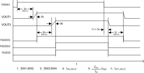
Figure 43 shows an example configuration in which both the SW1-SW2 pair and SW3-SW4 pair are current shared. The enable pin of the slave converter can either follow the master converter or be floating. For the PGOOD pin, the slave PGOOD follows the master PGOOD. Due to internal pull-ups to VDDD on ENSWx lines, the user has an option to control ENSWx if an always on condition is desired.
9.2.3 External Sequencing Application
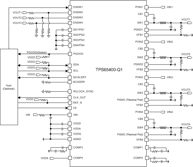
Figure 44 shows an example configuration where the VOUT outputs are linked to enable terminal ENSWx inputs in a daisy-chain configuration for start sequence SW1-SW2-SW3-SW4.
9.2.3.1 Design Requirements
Table 46 and Table 47 list PMBus commands to configure this device.
Table 46. PMBus Commands Used for External Sequencing through VOUT
| COMMAND NAME | CODE | NAME | BITS | COMMENT |
|---|---|---|---|---|
| PAGE | 00h | — | 7:0 | Selects output rail |
| STORE_DEFAULT_ALL | 11h | — | — | Save settings as default |
| PIN_CONFIG_00 | D2h | PGOOD_PIN_CONFIG(1) | 6:2 | PGOOD pin and of all PGOOD (manufacturer default) |
| ENABLE_PIN_CONFIG(1) | 1:0 | Active ENABLE (manufacturer default) | ||
| PIN_CONFIG_01 | D3h | SSPG_PIN_CONFIG(1) | 0 | Set to SSx for external soft-start (manufacturer default) |
| TON_TOFF_DELAY | DDh | TON_DELAY | 5:3 | Delay time before starting |
| TOFF_DELAY(1) | 2:0 | Delay time before stopping | ||
| RESET_DELAY | DCh | RESET_DELAY(1) | 2:0 | Reset delay time |
To achieve the timing requirements shown in Table 46, see Table 47 for an example configuration script.
Table 47. Example Configuration Script for External Sequencing through VOUT
| COMMAND NAME | CODE | WRITE BYTE | COMMENT |
|---|---|---|---|
| PAGE | 00h | 0xFF | Selects all |
| PIN_CONFIG_00(1) | D2h | 0x3C | Active ENABLE (manufacturer default) |
| RESET_DELAY(1) | DCh | 0x02 | 100-ms reset delay |
| PAGE | 00h | 0x00 | Selects SW1 |
| PIN_CONFIG_01(1) | D3h | 0x00 | Configure SS1/PG1 pin to SS1 for external soft-start |
| TON_TOFF_DELAY | DDh | 0x20 | 100-ms turn-on delay 0-ms turn-off delay |
| PAGE | 00h | 0x01 | Selects SW2 |
| PIN_CONFIG_01(1) | D3h | 0x00 | Configure SS2/PG2 pin to SS2 for external soft-start |
| TON_TOFF_DELAY | DDh | 0x20 | 100-ms turn-on delay 0-ms turn-off delay |
| PAGE | 00h | 0x02 | Selects SW3 |
| PIN_CONFIG_01(1) | D3h | 0x00 | Configure SS3/PG3 pin to SS3 for external soft-start |
| TON_TOFF_DELAY | DDh | 0x20 | 100-ms turn-on delay 0-ms turn-off delay |
| PAGE | 00h | 0x03 | Selects SW4 |
| PIN_CONFIG_01(1) | D3h | 0x00 | Configure SS4/PG4 pin to SS4 for external soft-start |
| TON_TOFF_DELAY | DDh | 0x20 | 100-ms turn-on delay 0-ms turn-off delay |
| STORE_DEFAULT_ALL | 11h | — | Save settings as default |
9.2.3.2 Detailed Design Procedure
9.2.3.2.1 External Sequencing Through PG Pins
In an application where the programmable soft-start ramping rate is sufficient and where stop sequencing is not required, it is possible to wire Power Good pins (global PGOOD, PG) to enable pins (ENSWx) according to the desired start sequence. This is useful in cases where multiple PMUs are configured and the PG or global PGOOD output of one PMU is required to turn on an output of another PMU.
9.2.3.2.2 External Sequencing Through SW
In an application where output voltages exceed the threshold voltage of the enable pins ENSWx, it is possible to wire a properly divided VOUT directly to the enable pins according to the desired start sequence.
9.2.3.2.3 Example Configuration
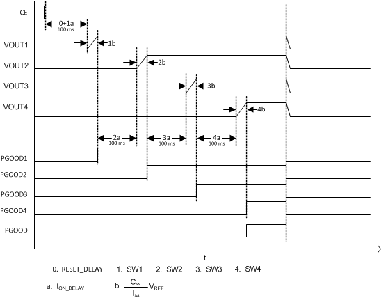 Figure 45. Example Timing Diagram for External Sequencing Through VOUT
NOTE
Only necessary if the defaults have been overwritten since device manufacture.