SLVSCY2A March 2015 – January 2016 TPS65632
PRODUCTION DATA.
- 1 Features
- 2 Applications
- 3 Description
- 4 Revision History
- 5 Pin Configuration and Functions
- 6 Specifications
-
7 Detailed Description
- 7.1 Overview
- 7.2 Functional Block Diagram
- 7.3 Feature Description
- 7.4 Device Functional Modes
- 8 Application and Implementation
- 9 Power Supply Recommendations
- 10Layout
- 11Device and Documentation Support
- 12Mechanical, Packaging, and Ordering Information
Package Options
Mechanical Data (Package|Pins)
- RTE|16
Thermal pad, mechanical data (Package|Pins)
- RTE|16
Orderable Information
8 Application and Implementation
NOTE
Information in the following applications sections is not part of the TI component specification, and TI does not warrant its accuracy or completeness. TI’s customers are responsible for determining suitability of components for their purposes. Customers should validate and test their design implementation to confirm system functionality.
8.1 Application Information
The TPS65632 device is intended to supply the main analog supplies required by AMOLED displays. VPOS is fixed at 4.6 V, but VNEG can be programmed using the CTRL pin to voltages in the range –1.4 V to –5.4 V. The SELP2 pin can be used to set AVDD to either 5.8 V or 7.7 V. The device is highly integrated and requires few external components.
8.2 Typical Application
Figure 8 shows a typical application circuit suitable for supplying AMOLED displays in smartphone applications. The circuit is designed to operate from a single-cell Li-Ion battery and generates a positive output voltage VPOS of 4.6 V, a negative output voltage VNEG of –4.0 V, and a positive output voltage AVDD of 5.8 V or 7.7 V. The VPOS and VNEG outputs are each capable of supplying up to 300 mA of current, and the AVDD output of up to 30 mA.
 Figure 8. Typical Application Circuit
8.2.1 Design Requirements
For this design example, use the parameters shown in Table 2
Table 2. Design Parameters
| PARAMETER | VALUE |
|---|---|
| Input voltage range | 2.9 V to 4.5 V |
| Output voltage | VPOS = 4.6 V VNEG = –4.0 V AVDD = 7.7 V |
| Current | I(VPOS) = 300 mA I(VNEG) = 300 mA I(AVDD) = 30 mA |
| Switching Frequency | f(SWP1) = 1.7 MHz f(SWN) = 1.7 MHz f(SWP2) = 1.7 MHz |
8.2.2 Detailed Design Procedure
In order to maximize performance, the TPS65632 device has been optimized for use with a relatively narrow range of component values, and customers are strongly recommended to use the application circuits shown in Figure 8 with the components listed in Table 3 and Table 4.
8.2.2.1 Inductor Selection
The VPOS and VNEG converters have been optimized for use with 4.7-µH inductors and the AVDD boost converter has been optimized for use with 10-µH inductors. For optimum performance it is recommended that these values be used in all applications. Customers using different inductors than the ones in Table 3 are strongly recommended to characterize circuit performance fully before finalizing their design. Customers should pay particular attention to the inductors' saturation current and ensure it is adequate for their application's worst-case conditions (which may also be during start-up).
Table 3. Inductor Selection
| REFERENCE DESIGNATOR | VALUE | MANUFACTURER | PART NUMBER |
|---|---|---|---|
| L1, L3 | 4.7 µH | Coilcraft | XFL4020-4R7ML |
| L2 | 10 µH | Coilmaster | MMPP252012-100N |
8.2.2.2 Capacitor Selection
The recommended capacitor values are shown in Table 4. Applications using less than the recommended capacitance (e.g. to save PCB area) may exhibit increased voltage ripple. In general, the lower the output current, the lower the necessary capacitance. Customers should be aware that ceramic capacitors of the kind typically used with the TPS65632 device exhibit dc bias effects, which means their effective capacitance under normal operating conditions may be significantly lower than their nominal capacitance value. Customers must ensure that the effective capacitance is sufficient for their application's performance requirements.
Table 4. Capacitor Selection
| REFERENCE DESIGNATOR | VALUE | MANUFACTURER | PART NUMBER |
|---|---|---|---|
| C1 | 3 × 10 µF | Murata | GRM21BR71A106KE51 |
| C2, C6 | 10 µF | Murata | GRM21BR71A106KE51 |
| C3 | 2 × 10 µF | Murata | GRM21BR71A106KE51 |
| C4, C5 | 100 nF | Murata | GRM155B11A104KA01 |
8.2.3 Application Curves
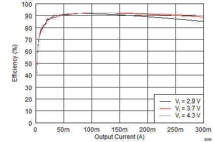
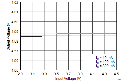
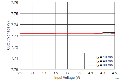
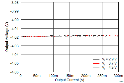
Unless otherwise stated: TA = 25°C, VI = 3.7 V, VPOS = 4.6 V, VNEG = –4.0 V, AVDD = 7.7 V; L1 = L3 = XFL4020-4R7ML, and L2 = MMPP252012-100N.
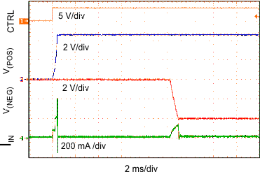
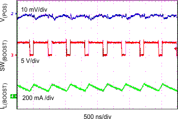
| IPOS = 100 mA | ||
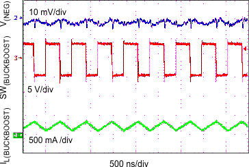
| INEG = 100 mA | ||

| IAVDD = 10 mA | ||
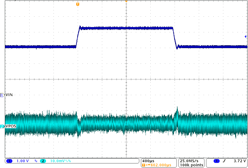
| VI = 3.0 V to 4.2 V in 50 µs | ||
| IPOS = 100 mA | ||

| VI = 3.0 V to 4.2 V in 50 µs | ||
| IAVDD = 30 mA | ||

| INEG = 10 mA to 100 mA in 100 ns | ||
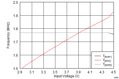
| IPOS = 100 mA | INEG = 100 mA | IAVDD = 30 mA |
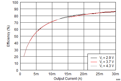
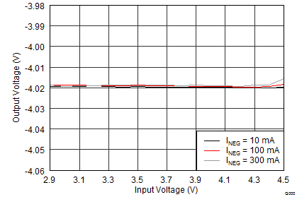
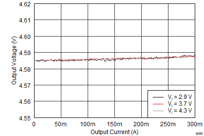
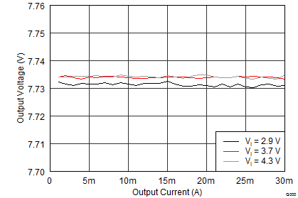
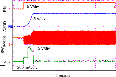

| IPOS = 300 mA | ||
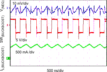
| INEG = 300 mA | ||
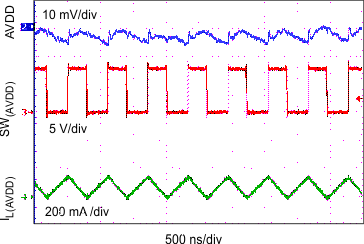
| IAVDD = 30 mA | ||
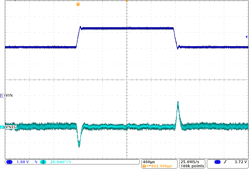
| VI = 3.0 V to 4.2 V in 50 µs | ||
| INEG = 100 mA | ||
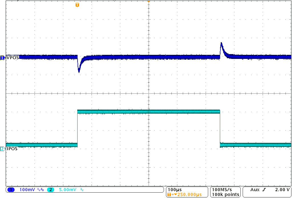
| IPOS = 10 mA to 100 mA in 100 ns | ||

| IAVDD = 10 mA to 30 mA in 100 ns | ||