SLVSCY2A March   2015  – January 2016 TPS65632

PRODUCTION DATA.  

  1. Features
  2. Applications
  3. Description
  4. Revision History
  5. Pin Configuration and Functions
  6. Specifications
    1. 6.1 Absolute Maximum Ratings
    2. 6.2 ESD Ratings
    3. 6.3 Recommended Operating Conditions
    4. 6.4 Thermal Information
    5. 6.5 Electrical Characteristics
    6. 6.6 Timing Requirements
    7. 6.7 Typical Characteristics
  7. Detailed Description
    1. 7.1 Overview
    2. 7.2 Functional Block Diagram
    3. 7.3 Feature Description
      1. 7.3.1 Boost Converter 1 (VPOS)
        1. 7.3.1.1 V(POS) Boost Output Sense (FBS Pin)
      2. 7.3.2 Inverting Buck-Boost Converter (VNEG)
        1. 7.3.2.1 Programming VNEG
        2. 7.3.2.2 Controlling VNEG Transition Time
      3. 7.3.3 Boost Converter 2 (AVDD)
      4. 7.3.4 Soft Start and Start-Up Sequence
      5. 7.3.5 Enable (CTRL)
      6. 7.3.6 Undervoltage Lockout
      7. 7.3.7 Short-Circuit Protection
        1. 7.3.7.1 Short Circuits During Operation
        2. 7.3.7.2 Short Circuits During Start Up
      8. 7.3.8 Output Discharge During Shut Down
      9. 7.3.9 Thermal Shutdown
    4. 7.4 Device Functional Modes
      1. 7.4.1 Operation with VI < 2.9 V
      2. 7.4.2 Operation with VI ≈ VPOS (Diode Mode)
      3. 7.4.3 Operation with CTRL
  8. Application and Implementation
    1. 8.1 Application Information
    2. 8.2 Typical Application
      1. 8.2.1 Design Requirements
      2. 8.2.2 Detailed Design Procedure
        1. 8.2.2.1 Inductor Selection
        2. 8.2.2.2 Capacitor Selection
      3. 8.2.3 Application Curves
  9. Power Supply Recommendations
  10. 10Layout
    1. 10.1 Layout Guidelines
    2. 10.2 Layout Example
  11. 11Device and Documentation Support
    1. 11.1 Device Support
      1. 11.1.1 Third-Party Products Disclaimer
    2. 11.2 Trademarks
    3. 11.3 Electrostatic Discharge Caution
    4. 11.4 Glossary
  12. 12Mechanical, Packaging, and Ordering Information

Package Options

Mechanical Data (Package|Pins)
Thermal pad, mechanical data (Package|Pins)
Orderable Information

10 Layout

10.1 Layout Guidelines

  • Place the input capacitor on PVIN and the output capacitor on OUTN as close as possible to device. Use short and wide traces to connect the input capacitor on PVIN and the output capacitor on OUTN.
  • Place the output capacitor on OUTP1 and OUTP2 as close as possible to device. Use short and wide traces to connect the output capacitor on OUTP1 and OUTP2.
  • Connect the ground of CT capacitor with AGND, pin 7, directly.
  • Connect input ground and output ground on the same board layer, not through via hole.
  • Connect AGND, PGND1 and PGND2 with exposed thermal pad.

10.2 Layout Example
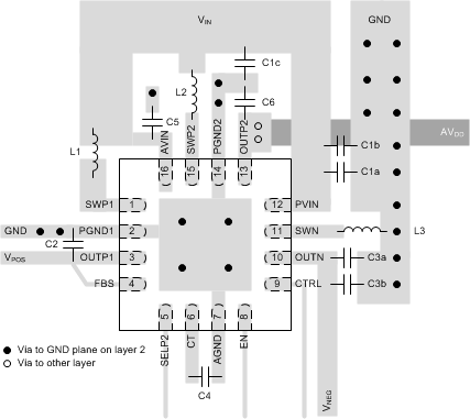
TPS65632 layout_slvscy2.gif Figure 32. Recommended PCB Layout