SLVSCY2A March   2015  – January 2016 TPS65632

PRODUCTION DATA.  

  1. Features
  2. Applications
  3. Description
  4. Revision History
  5. Pin Configuration and Functions
  6. Specifications
    1. 6.1 Absolute Maximum Ratings
    2. 6.2 ESD Ratings
    3. 6.3 Recommended Operating Conditions
    4. 6.4 Thermal Information
    5. 6.5 Electrical Characteristics
    6. 6.6 Timing Requirements
    7. 6.7 Typical Characteristics
  7. Detailed Description
    1. 7.1 Overview
    2. 7.2 Functional Block Diagram
    3. 7.3 Feature Description
      1. 7.3.1 Boost Converter 1 (VPOS)
        1. 7.3.1.1 V(POS) Boost Output Sense (FBS Pin)
      2. 7.3.2 Inverting Buck-Boost Converter (VNEG)
        1. 7.3.2.1 Programming VNEG
        2. 7.3.2.2 Controlling VNEG Transition Time
      3. 7.3.3 Boost Converter 2 (AVDD)
      4. 7.3.4 Soft Start and Start-Up Sequence
      5. 7.3.5 Enable (CTRL)
      6. 7.3.6 Undervoltage Lockout
      7. 7.3.7 Short-Circuit Protection
        1. 7.3.7.1 Short Circuits During Operation
        2. 7.3.7.2 Short Circuits During Start Up
      8. 7.3.8 Output Discharge During Shut Down
      9. 7.3.9 Thermal Shutdown
    4. 7.4 Device Functional Modes
      1. 7.4.1 Operation with VI < 2.9 V
      2. 7.4.2 Operation with VI ≈ VPOS (Diode Mode)
      3. 7.4.3 Operation with CTRL
  8. Application and Implementation
    1. 8.1 Application Information
    2. 8.2 Typical Application
      1. 8.2.1 Design Requirements
      2. 8.2.2 Detailed Design Procedure
        1. 8.2.2.1 Inductor Selection
        2. 8.2.2.2 Capacitor Selection
      3. 8.2.3 Application Curves
  9. Power Supply Recommendations
  10. 10Layout
    1. 10.1 Layout Guidelines
    2. 10.2 Layout Example
  11. 11Device and Documentation Support
    1. 11.1 Device Support
      1. 11.1.1 Third-Party Products Disclaimer
    2. 11.2 Trademarks
    3. 11.3 Electrostatic Discharge Caution
    4. 11.4 Glossary
  12. 12Mechanical, Packaging, and Ordering Information

Package Options

Mechanical Data (Package|Pins)
Thermal pad, mechanical data (Package|Pins)
Orderable Information

6 Specifications

6.1 Absolute Maximum Ratings

over operating free-air temperature range (unless otherwise noted)(1)
MIN MAX UNIT
Input supply voltage(2) SWP1, OUTP1, FBS, PVIN, AVIN –0.3 5 V
SWP2 –0.3 12 V
OUTP2 –0.3 8.5 V
OUTN –6.0 0.3 V
SWN –6.5 4.8 V
CTRL, EN, SELP2 –0.3 5.5 V
CT –0.3 3.6 V
Operating virtual junction, TJ –40 150 °C
Storage temperature, Tstg –65 150 °C
(1) Stresses beyond those listed under absolute maximum ratings may cause permanent damage to the device. These are stress ratings only, and functional operation of the device at these or any other conditions beyond those indicated under recommended operating conditions is not implied. Exposure to absolute-maximum-rated conditions for extended periods my affect device reliability.
(2) With respect to GND pin.

6.2 ESD Ratings

VALUE UNIT
V(ESD) Electrostatic discharge Human body model (HBM), per ANSI/ESDA/JEDEC JS-001, all pins(1) ±2000 V
Charged device model (CDM), per JEDEC specification JESD22-C101, all pins(2) ±500
(1) JEDEC document JEP155 states that 500-V HBM allows safe manufacturing with a standard ESD control process.
(2) JEDEC document JEP157 states that 250-V CDM allows safe manufacturing with a standard ESD control process.

6.3 Recommended Operating Conditions

over operating free-air temperature range (unless otherwise noted)
MIN NOM MAX UNIT
INPUT
VI Input supply voltage range 2.9 3.7 4.5 V
TJ Operating junction temperature –40 85 125 °C

6.4 Thermal Information

THERMAL METRIC(1) RTE [WQFN] UNIT
16 PINS
RθJA Junction-to-ambient thermal resistance 42.9 °C/W
RθJC(top) Junction-to-case (top) thermal resistance 44
RθJB Junction-to-board thermal resistance 14.2
ψJT Junction-to-top characterization parameter 0.6
ψJB Junction-to-board characterization parameter 14.1
RθJC(bot) Junction-to-case (bottom) thermal resistance 3.3
(1) For more information about traditional and new thermal metrics, see the IC Package Thermal Metrics application report, SPRA953.

6.5 Electrical Characteristics

VI = 3.7 V, CTRL = 3.7 V, EN = 3.7 V, VPOS = 4.6 V, VNEG = –4.0 V, AVDD = 7.7 V, TJ = –40°C to 85°C, typical values are at TJ = 25°C (unless otherwise noted)
PARAMETER TEST CONDITIONS MIN TYP MAX UNIT
SUPPLY CURRENT AND THERMAL PROTECTION
VI Input voltage range 2.9 3.7 4.5 V
ISD Shutdown current CTRL = GND, EN = GND, sum of current flowing into AVIN and PVIN 0.25 5 µA
VUVLO Under-voltage lockout threshold VI falling 1.8 2.1 V
VI rising 2.1 2.5 V
BOOST CONVERTER 1 (VPOS)
VPOS Positive output 1 voltage 4.6 V
Positive output 1 voltage variation 25°C ≤ TA ≤ 85°C, No load –0.5% 0.5%
–30°C ≤ TA ≤ 85°C, No load –0.8% 0.8%
rDS(on)1A Switch on-resistance I(SWP1) = 200 mA 200
rDS(on)1B Rectifier on-resistance 350
fSW1 Switching frequency IPOS = 200mA 1.7 MHz
ISW1 Switch current limit Inductor valley current 0.8 1 1.4 A
VSCP1 Short-circuit threshold in operation VPOS falling 3.95 4.10 4.28 V
tSCP1 Short-circuit detection time in operation 3 ms
VT Output voltage sense threshold V(OUTP1) – V(FBS) increasing 200 300 550 mV
V(OUTP1) – V(FBS) decreasing 100 200 450 mV
R(FBS) FBS pin pull-down resistance 2 4 6
RDCHG1 Discharge resistance CTRL = GND, I(SWP1) = 1mA 10 30 70 Ω
Line regulation IPOS = 200mA 0.01 %/V
Load regulation 1 mA ≤ IPOS ≤ 300 mA 0.007 %/A
INVERTING BUCK-BOOST CONVERTER (VNEG)
VNEG Output voltage default –4.0 V
Output voltage range –1.4 –5.4
Output voltage accuracy 25°C ≤ TA ≤ 85°C, no load –50 50 mV
–30°C ≤ TA ≤ 85°C, no load –60 60
rDS(on)2A SWN MOSFET on-resistance I(SWN) = 200 mA 200
rDS(on)2B SWN MOSFET rectifier on-resistance 300
fSW2 SWN Switching frequency INEG = 10 mA 1.7 MHz
ISW2 SWN switch current limit VI = 2.9 V 1.5 2.2 3 A
VSCP2 Short circuit threshold in operation Voltage increase from nominal VNEG 300 500 700 mV
Short circuit threshold in start up 180 200 230 mV
tSCP2 Short circuit detection time in start up 10 ms
Short circuit detection time in operation 3 ms
RDCHG2 Discharge resistance CTRL = GND, I(SWN) = 1 mA 130 150 170 Ω
Line regulation INEG = 200 mA 0.004 %/V
Load regulation 0.1 %/A
BOOST CONVERTER 2 (AVDD)
AVDD Output voltage SELP2 = Low 7.7 V
SELP2 = High 5.8
Output voltage accuracy 25°C ≤ TA ≤ 85°C, no load –1% 1%
–30°C ≤ TA ≤ 85°C, no load –1.3% 1.3%
rDS(on)3A SWP2 switch on-resistance I(SWP2) = 200 mA 400
rDS(on)3B SWP2 rectifier on-resistance 650
fSW3 Switching frequency IAVDD = 0 mA 1.7 MHz
ILIM3 Switch current limit Inductor valley current 0.25 0.35 0.45 A
RDCHG3 Discharge resistance EN = GND, I(SWP2) = 1 mA 10 30 70 Ω
Line regulation IAVDD = 30 mA 0.02 %/V
Load regulation 0.18 %/A
CTRL INTERFACE (CTRL, EN, SELP2)
VIH Logic input high level voltage 1.2 V
VIL Logic input low level voltage 0.4 V
R Pull-down resistance 150 400 860
OTHER
RCT CT pin resistance 150 300 500
tINIT Initialization time 300 400 µs
tSTORE Data storage/accept time period 30 80 µs
tSDN Shutdown time period 30 80 µs
TSD Thermal shutdown temperature Temperature rising 145 °C

6.6 Timing Requirements

MIN NOM MAX UNIT
CTRL INTERFACE
tLOW Low-level pulse duration 2 10 25 µs
tHIGH High-level pulse duration 2 10 25 µs
tOFF Shutdown pulse duration (CTRL = low) 200 µs

6.7 Typical Characteristics

TJ = 25°C, VI = 3.7 V, unless otherwise stated.
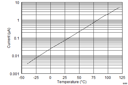
TPS65632 isd_vs_temp_slvscy2.png
Figure 1. Shutdown Current into AVIN and PVIN Pins
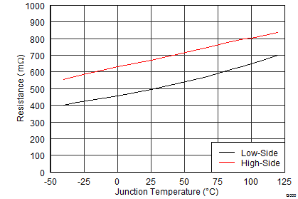
TPS65632 vneg_rdson_vs_temp_slvscy2.png
Figure 3. Inverting Buck-Boost Converter (VNEG) rDS(ON)
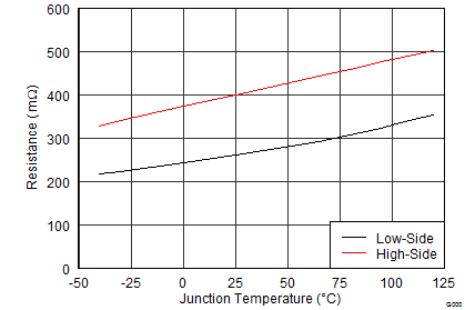
TPS65632 vpos_rdson_vs_temp_slvscy2.png
Figure 2. Boost Converter 1 (VPOS) rDS(ON)
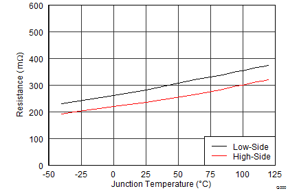
TPS65632 avdd_rdson_vs_temp_slvscy2.png
Figure 4. Boost Converter 2 (AVDD) rDS(ON)