SLVSA08A February 2010 – September 2015 TPS657052
PRODUCTION DATA.
- 1 Features
- 2 Applications
- 3 Description
- 4 Revision History
- 5 Device Options
- 6 Pin Configuration and Functions
- 7 Specifications
- 8 Detailed Description
- 9 Application and Implementation
- 10Power Supply Recommendations
- 11Layout
- 12Device and Documentation Support
- 13Mechanical, Packaging, and Orderable Information
Package Options
Mechanical Data (Package|Pins)
- YZH|16
Thermal pad, mechanical data (Package|Pins)
Orderable Information
7 Specifications
7.1 Absolute Maximum Ratings
over operating free-air temperature range (unless otherwise noted)| MIN | MAX | UNIT | ||
|---|---|---|---|---|
| Input voltage on all pins except A/PGND pins with respect to AGND | –0.3 | 7 | V | |
| Voltage on pin VLDO1 with respect to AGND | –0.3 | 3.6 | V | |
| Current | L1, VLDO1, VINLDO1, PGND | 600 | mA | |
| AGND | 20 | mA | ||
| All other pins | 3 | mA | ||
| Continuous total power dissipation | See Dissipation Ratings | |||
| Operating free-air temperature, TA | –40 | 85 | °C | |
| Maximum junction temperature, TJ | 125 | °C | ||
| Storage temperature, Tstg | –65 | 150 | °C | |
7.2 ESD Ratings
| VALUE | UNIT | ||||
|---|---|---|---|---|---|
| V(ESD) | Electrostatic discharge | Human body model (HBM), per ANSI/ESDA/JEDEC JS-001(1) | ±2000 | V | |
| Charged device model (CDM), per JEDEC specification JESD22-C101(2) | ±500 | ||||
(1) JEDEC document JEP155 states that 500-V HBM allows safe manufacturing with a standard ESD control process.
(2) JEDEC document JEP157 states that 250-V CDM allows safe manufacturing with a standard ESD control process.
7.3 Recommended Operating Conditions
over operating free-air temperature range (unless otherwise noted)| MIN | NOM | MAX | UNIT | ||
|---|---|---|---|---|---|
| VIN1/2 | Input voltage for step-down converter DCDC1 and DCDC2 | 3.3 | 6 | V | |
| IOUTDCDC1/2 | Output current at L | 400 | mA | ||
| L | Inductor at L | 1.5 | 2.2 | 4.7 | µH |
| VINLDO | Input voltage for LDO | 1.7 | 6.0 | V | |
| ILDO | Output current at LDO | 200 | mA | ||
| CINDCDC1/2 | Input Capacitor at VIN1 and VIN2 | 4.7 | µF | ||
| COUTDCDC1/2 | Output Capacitor at VOUT1, VOUT2 | 4.7 | 10 | 22 | µF |
| CINLDO | Input Capacitor at VINLDO | 2.2 | µF | ||
| COUTLDO | Output Capacitor at VLDO | 2.2 | µF | ||
| TA | Operating ambient temperature | –40 | 85 | °C | |
| TJ | Operating junction temperature | –40 | 125 | °C | |
7.4 Thermal Information
| THERMAL METRIC(1) | TPS65705x | UNIT | |
|---|---|---|---|
| YZH (DSBGA) | |||
| 16 PINS | |||
| RθJA | Junction-to-ambient thermal resistance | 75 | °C/W |
| RθJC(top) | Junction-to-case (top) thermal resistance | 22 | °C/W |
| RθJB | Junction-to-board thermal resistance | 26 | °C/W |
| ψJT | Junction-to-top characterization parameter | 0.2 | °C/W |
| ψJB | Junction-to-board characterization parameter | 24 | °C/W |
| RθJC(bot) | Junction-to-case (bottom) thermal resistance | N/A | °C/W |
(1) For more information about traditional and new thermal metrics, see the Semiconductor and IC Package Thermal Metrics application report, SPRA953.
7.5 Electrical Characteristics
Unless otherwise noted: VIN1 = VIN2 = VINLDO = 3.6 V, L = LQMP21P 2.2 µH, COUTDCDCx = 10 µF, COUTLDO = 2.2 µF, TA = –40°C to +85°C| PARAMETER | TEST CONDITIONS | MIN | TYP | MAX | UNIT | |
|---|---|---|---|---|---|---|
| SUPPLY CURRENT | ||||||
| IQ | Operating quiescent current DCDCx | DCDC1 and DCDC2 enabled, IOUT = 0 mA, MODE =0 (PFM mode), LDO disabled |
40 | µA | ||
| DCDC1 or DCDC2 enabled, IOUT = 0 mA, MODE =0 (PFM mode), LDO disabled |
25 | µA | ||||
| DCDC1 or DCDC2 enabled, IOUT = 0 mA. MODE =1 (forced PWM mode), LDO disabled | 4 | mA | ||||
| Operating quiescent current LDO | DCDC1 and DCDC2 disabled, LDO enabled. IOUT = 0 mA |
25 | 37 | µA | ||
| ISD | Shutdown current | DCDC1, DCDC2, and LDO disable | 5 | 12 | µA | |
| DIGITAL PINS (EN1, EN2, ENLDO, MODE) | ||||||
| VIH | High-level input voltage for EN1, EN2, ENLDO, MODE | 1.2 | VCC | V | ||
| VIL | Low-level input voltage for EN1, EN2, ENLDO, MODE | 0.4 | V | |||
| ILKG | Input leakage current | EN1, EN2, ENLDO, MODE tied to GND or VIN = VIN2 |
0.01 | 0.1 | μA | |
| STEP-DOWN CONVERTERS | ||||||
| VIN1 | Input voltage for DCDC1 | 3.3 | 6 | V | ||
| VIN2 | Input voltage for DCDC2 | 3.3 | 6 | V | ||
| UVLO | Internal undervoltage lockout threshold | VIN1 = VIN2 falling | 2.15 | 2.2 | 2.25 | V |
| Internal undervoltage lockout threshold hysteresis | VIN1 = VIN2 rising | 120 | mV | |||
| POWER SWITCH | ||||||
| RDS(ON) | High-side MOSFET ON-resistance | VIN1 = VIN2 = 3.6 V | 350 | 750 | mΩ | |
| Low-side MOSFET ON-resistance | VIN1 = VIN2 = 3.6 V | 350 | 600 | mΩ | ||
| ILIMF | Forward current limit | 3.3 V ≤ VIN1 = VIN2 ≤ 6 V | 550 | 650 | 770 | mA |
| IOUTDCDC1/2 | DCDC1/DCDC2 output current | VIN1 = VIN2 > 3.3 V , L = 2.2 µH | 400 | mA | ||
| OSCILLATOR | ||||||
| fSW | Oscillator frequency | 2.03 | 2.25 | 2.48 | MHz | |
| OUTPUT | ||||||
| VOUT1 | DCDC1 default output voltage | VIN1 = VIN2 ≥ 3.3 V | 3.3 | V | ||
| VOUT2 | DCDC2 default output voltage | VIN1 = VIN2 ≥ 3.3 V | 1.8 | V | ||
| IFB | FB pin input current | DC-DC converter disabled | 0.1 | µA | ||
| VOUT | DC output voltage accuracy(1) | VIN1 = VIN2 = 3.3 V to 6 V, +1% voltage positioning active; PFM operation, 0 mA < IOUT < IOUTMAX | +1% | +3% | ||
| DC output voltage accuracy | VIN1 = VIN2 = 3.3 V to 6 V, PWM operation, 0 mA < IOUT < IOUTMAX |
–1.5% | +1.5% | |||
| DC output voltage load regulation | PWM operation | 0.5 | %/A | |||
| tStart | Start-up time | Time from active EN to Start switching | 200 | µs | ||
| tRamp | VOUT ramp time | Time to ramp from 5% to 95% of VOUT | 250 | µs | ||
| RDIS | Internal discharge resistor at L1 or L2 (TPS657051 Only) |
DCDC1 or DCDC2 disabled | 250 | 400 | 600 | Ω |
| THERMAL PROTECTION SEPARATELY FOR DCDC1, DCDC2 AND LDO1 | ||||||
| TSD | Thermal shutdown | Increasing junction temperature | 150 | °C | ||
| Thermal shudown hysteresis | Decreasing junction temperature | 30 | °C | |||
| VLDO, LOW DROPOUT REGULATOR | ||||||
| VINLDO | Input voltage range for LDO | 1.7 | 6 | V | ||
| VLDO | TPS657051 LDO default output voltage(2) | 3 | V | |||
| VLDO | TPS657052 LDO default output voltage(3) | 2.8 | V | |||
| IO | Output current for LDO | 200 | mA | |||
| ISC | LDO short circuit current limit | VLDO = GND | 340 | 400 | 550 | mA |
| Dropout voltage at LDO | IO = 200 mA | 200 | mV | |||
| Output voltage accuracy for LDO | IO = 100 mA, VOUT = 2.8V | –2% | +2% | |||
| Line regulation for LDO | VINLDO = VLDO + 0.5 V (min. 1.7 V) to 6 V, IO = 50 mA |
–1% | 1% | |||
| Load regulation for LDO | IO = 1 mA to 200 mA for LDO | –1% | 1% | |||
| PSRR | Power supply rejection ratio | fNOISE ≤ 10 kHz, COUT ≥ 2.2 µf Vin = 5 V, Vout = 2.8 V, IOUT = 100 mA |
50 | dB | ||
| Vn | Ouput noise voltage | Vout = 2.8 V, BW = 10Hz to 100kHz | 160 | µV RMS | ||
| tRamp | VOUT ramp time | Internal soft-start when LDO is enabled; Time to ramp from 5% to 95% of VOUT | 200 | µs | ||
| RDIS | Internal discharge resistor at VLDO | LDO disabled | 250 | 400 | 550 | Ω |
(1) In Power Save Mode (PFM), the internal reference voltage is 1.01 × Vref.
(2) VINLDO > 3 V
(3) VINLDO > 2.8 V
7.6 Dissipation Ratings
| DEVICE | PACKAGE | RθJA | TA ≤ 25°C POWER RATING |
DERATING FACTOR ABOVE TA = 25°C |
TA = 70°C POWER RATING |
TA = 85°C POWER RATING |
|---|---|---|---|---|---|---|
| TPS657051/52(1) | YZH | 185 | 540 mW | 5.4 mW | 297 mW | 216 mW |
| TPS657051/52(2) | YZH | 75 | 1.3 W | 13.3 mW | 0.7 W | 0.5 W |
(1) The JEDEC low-K (1s) board used to derive this data was a 3in × 3in, two-layer board with 2-ounce copper traces on top of the board.
(2) The JEDEC high-K (2s2p) board used to derive this data was a 3in × 3in, multilayer board with 1-ounce internal power and ground.
7.7 Typical Characteristics
Table 1. Table Of Graphs
| FIGURE | ||
|---|---|---|
| Efficiency DC-DC (VDCDC= 3.3 V), L = BRC1608 1.5 µH | vs Load current / PFM mode | Figure 1 |
| Efficiency DC-DC (VDCDC= 3.3 V), L = BRC1608 1.5 µH | vs Load current / PWM mode | Figure 2 |
| Efficiency DC-DC (VDCDC= 1.8 V), L = BRC1608 1.5 µH | vs Load current / PFM mode | Figure 3 |
| Efficiency DC-DC (VDCDC= 1.8 V), L = BRC1608 1.5 µH | vs Load current / PWM mode | Figure 4 |
| Line transient response DC-DC 1.8 V (PWM) | Scope plot | Figure 5 |
| Line transient response DC-DC 1.8 V (PFM) | Scope plot | Figure 6 |
| Line transient response LDO 2.8 V | Scope plot | Figure 7 |
| Load transient response DC-DC 1.8 V (PWM/PFM) 20 mA to 180 mA |
Scope plot | Figure 8 |
| Load transient response DC-DC 1.8 V (PWM) 20 mA to 180 mA | Scope plot | Figure 9 |
| Load transient response DC-DC 1.8 V (PFM/PWM) 20 mA to 360 mA |
Scope plot | Figure 10 |
| Load transient response DC-DC 1.8 V (PWM) 20 mA to 360 mA | Scope plot | Figure 11 |
| Load transient response LDO 2.8 V | Scope plot | Figure 12 |
| DC-DC PFM to PWM mode transition | Scope plot | Figure 13 |
| DC-DC PWM to PFM mode transition | Scope plot | Figure 14 |
| DC-DC Output voltage ripple in PFM mode | Scope plot | Figure 15 |
| DC-DC Output voltage ripple in PWM mode | Scope plot | Figure 16 |
| Startup timing DC-DC 1.8 V | Scope plot | Figure 22 |
| Startup timing LDO 2.8 V | Scope plot | Figure 23 |
| LDO PSRR | Scope plot | Figure 17 |
| DC-DC Quiescent current | vs VINDCDC | Figure 18 |
| LDO Quiescent current | vs VINDCDC | Figure 19 |
| Shutdown current | vs VINDCDC | Figure 20 |
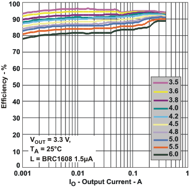 Figure 1. Efficiency DC-DC (VDCDC=3.3 V) vs Load Current PFM Mode
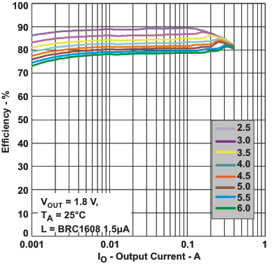 Figure 3. Efficiency DC-DC (VDCDC=1.8 V) vs Load Current PFM mode
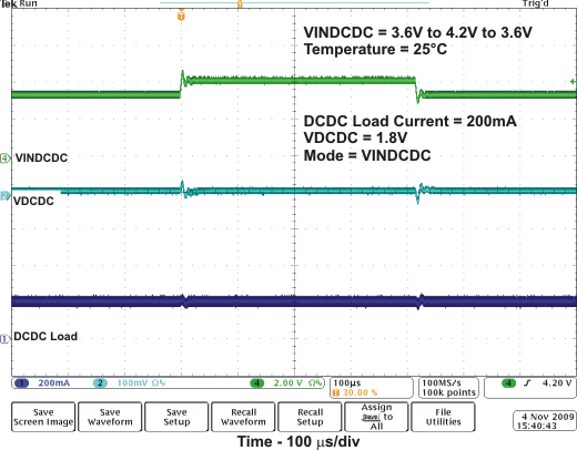 Figure 5. Line Transient Response DC-DC 1.8 V (PWM)
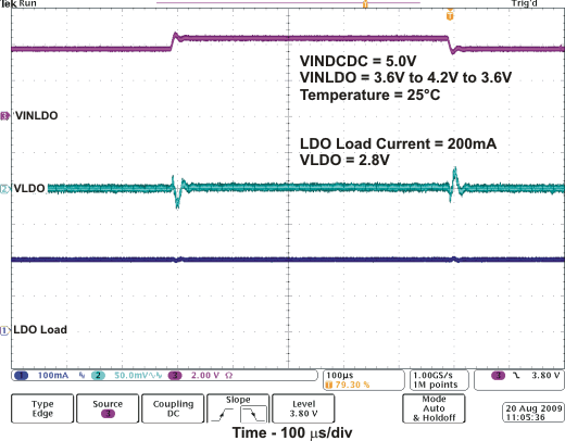 Figure 7. Line Transient Response LDO 2.8 V
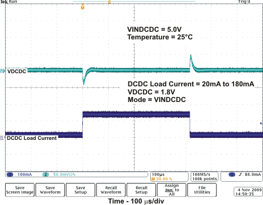 Figure 9. Load Transient Response DC-DC 1.8 V (PWM)
20 mA to 180 mA
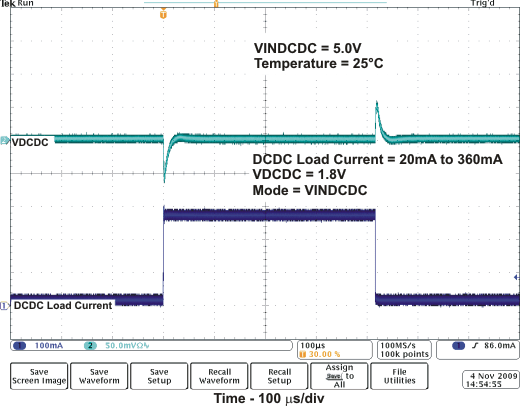 Figure 11. Load Transient Response DC-DC 1.8 V (PWM)
 20 mA to 360 mA
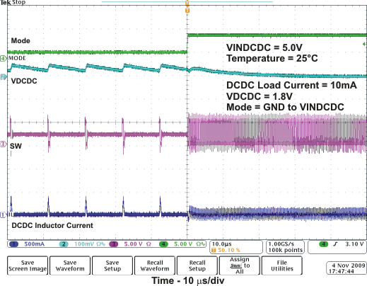 Figure 13. DC-DC PFM to PWM Mode Transition
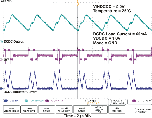 Figure 15. DC-DC Output Voltage Ripple in PFM Mode
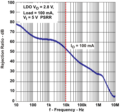 Figure 17. LDO PSRR
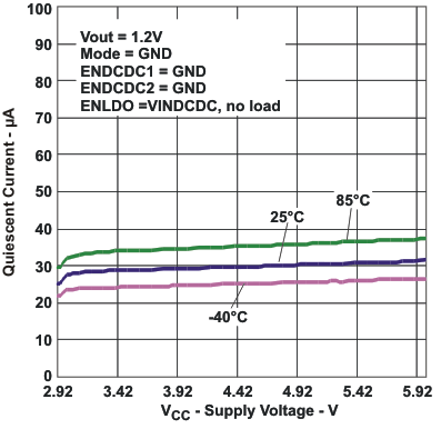 Figure 19. LDO Quiescent Current
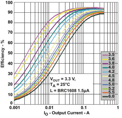 Figure 2. Efficiency DC-DC (VDCDC=3.3 V) vs Load Current PWM Mode
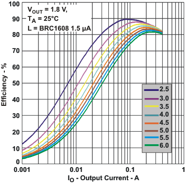 Figure 4. Efficiency DC-DC (VDCDC=1.8 V) vs Load Current PWM mode
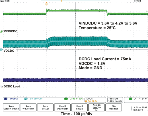 Figure 6. Line Transient Response DC-DC 1.8 V (PFM)
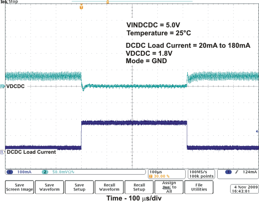 Figure 8. Load Transient Response DC-DC 1.8 V (PWM/PFM) 20 mA to 180 mA
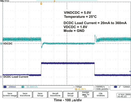 Figure 10. Load Transient Response DC-DC 1.8 V (PFM/PWM) 20 mA to 360 mA
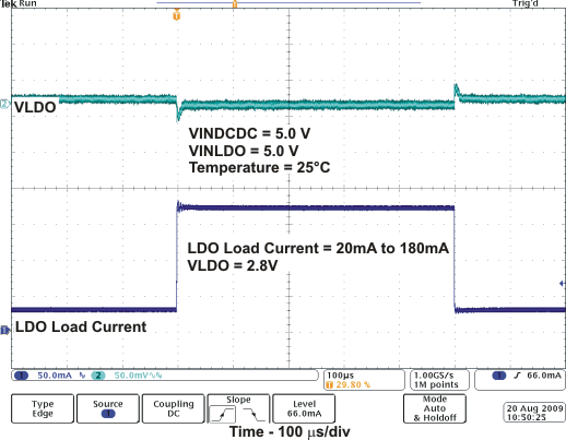 Figure 12. Load Transient Response LDO
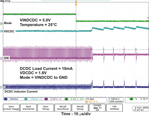 Figure 14. DC-DC PWM to PFM Mode Transition
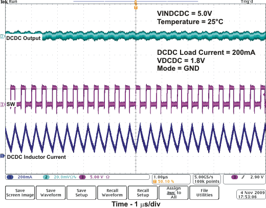 Figure 16. DC-DC Output Voltage Ripple in PWM Mode
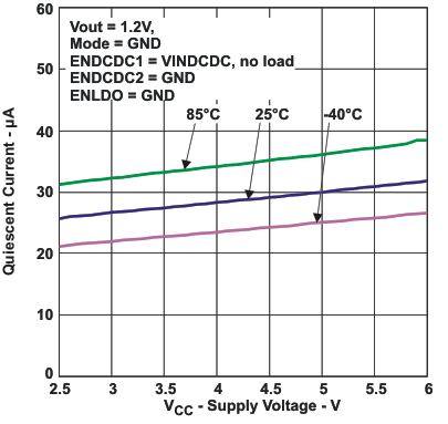 Figure 18. DC-DC Quiescent Current
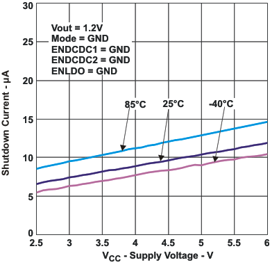 Figure 20. Shutdown Current