SWCS106F March 2013 – July 2016 TPS659119-Q1
PRODUCTION DATA.
- 1 Features
- 2 Applications
- 3 Description
- 4 Revision History
- 5 Description (continued)
- 6 Pin Configuration and Functions
-
7 Specifications
- 7.1 Absolute Maximum Ratings
- 7.2 ESD Ratings
- 7.3 Recommended Operating Conditions
- 7.4 Thermal Characteristics
- 7.5 External Component Recommendation
- 7.6 I/O Pullup and Pulldown Characteristics
- 7.7 Digital I/O Voltage Electrical Characteristics
- 7.8 I2C Interface and Control Signals
- 7.9 Switching Characteristics—I2C Interface and Control Signals
- 7.10 Power Consumption
- 7.11 Power References and Thresholds
- 7.12 Thermal Monitoring and Shutdown
- 7.13 32-kHz RTC Clock
- 7.14 VRTC LDO
- 7.15 VIO SMPS
- 7.16 VDD1 SMPS
- 7.17 VDD2 SMPS
- 7.18 EXTCTRL
- 7.19 LDO1 AND LDO2
- 7.20 LDO3 and LDO4
- 7.21 LDO5
- 7.22 LDO6 and LDO7
- 7.23 LDO8
- 7.24 Timing Requirements for Boot Sequence Example
- 7.25 Power Control Timing Requirements
- 7.26 Device SLEEP State Control Timing Requirements
- 7.27 Supplies State Control Through EN1 and EN2 Timing Characteristics
- 7.28 VDD1 Supply Voltage Control Through EN1 Timing Requirements
- 7.29 Typical Characteristics
- 8 Detailed Description
- 9 Application and Implementation
- 10Power Supply Recommendations
- 11Layout
- 12Device and Documentation Support
- 13Mechanical, Packaging, and Orderable Information
Package Options
Mechanical Data (Package|Pins)
- PFP|80
Thermal pad, mechanical data (Package|Pins)
- PFP|80
Orderable Information
9 Application and Implementation
NOTE
Information in the following applications sections is not part of the TI component specification, and TI does not warrant its accuracy or completeness. TI’s customers are responsible for determining suitability of components for their purposes. Customers should validate and test their design implementation to confirm system functionality.
9.1 Application Information
The TPS659119-Q1 device is an integrated power-management integrated circuit (PMIC) that comes in an 80-pin, 0.5-mm pitch, LQFP package with thermal pad. This device was designed specifically for automotive applications and is dedicated to designs powered from a 5-V input supply that require multiple power rails. The device provides three step-down converters along with an interface to control an external converter and eight LDO regulators. The device can support a variety of different processors and applications. Two of the step-down converters support dynamic voltage scaling through a dedicated I2C interface to provide optimum power savings. The third converter provides power for the I/Os and memory in the system.
In addition to the power resources, the device contains an embedded power controller (EPC) to manage the power sequencing requirements of systems. The power sequencing is programmable through EEPROM. The device also contains nine configurable GPIOs, a real-time clock module, an internal watchdog circuit, and two LED ON and OFF signal generators.
Details on how to use this device in automotive applications are described throughout this device specification. The following sections provide the typical application use-case with the recommended external components and layout guidelines.
9.2 Typical Application
Following the typical application schematic (see Figure 25) and the list of recommended external components will allow the TPS659119-Q1 device to achieve accurate and stable regulation with the step-down converters and LDO regulators. These devices are internally compensated and have been designed to operate most effectively with the component values listed in Table 91. Deviating from these values is possible but is not recommended.
9.2.1 Design Requirements
For this design example, use the parameters listed in Table 91.
Table 91. Design Parameters
| REFERENCE DESIGNATOR | COMPONENT FUNCTION | VALUE(1) |
|---|---|---|
| C1 | Input-supply decoupling capacitor | 4.7 µF, 10 V |
| C2 | VRTC output capacitor | 2.2 µF, 6.3 V |
| C3 | Crystal load capacitors | 10 pF, 50 V |
| C4 | ||
| C5 | VREF filtering capacitor | 100 nF |
| C6 | LDO output capacitors | 2.2 µF, 6.3 V |
| C7 | ||
| C8 | ||
| C16 | ||
| C17 | ||
| C18 | ||
| C19 | ||
| C20 | ||
| C9 | Step-down converter input capacitors | 10 µF, 10 V |
| C11 | ||
| C14 | ||
| C10 | Step-down converter output capacitors | 10 µF, 10 V |
| C12 | ||
| C15 | ||
| C13 | External-converter output capacitor | 22 µF, 10 V (×2) |
| L1 | Step-down converter inductors | 2.2 µH, 2.6 A |
| L2 | ||
| L3 | ||
| L4 | ||
| Y1 | Crystal | 16.384 MHz |
9.2.2 Detailed Design Procedure
9.2.2.1 Step-down Converter Input Capacitors
All step-down converter inputs require an input decoupling capacitor to minimize input ripple voltage. Using a 10-V, 10-µF capacitor for each step-down converter input is recommended. Depending on the input voltage of the step-down converter, a 6.3-V or 10-V capacitor can be used.
For optimal performance, the input capacitors should be placed as close to the step-down converter-input pins as possible. See the Layout Guidelines section for more information about component placement.
9.2.2.2 Step-down Converter Output Capacitors
All step-down converter outputs require an output capacitor to hold up the output voltage during a load step or a change to the input voltage. To ensure stability across the entire switching frequency range, the TPS659119-Q1 device requires an output capacitance value between 4 µF and 12 µF. To meet this requirement across temperature and DC bias voltage, using a 10-µF capacitor for each step-down converter is recommended.
9.2.2.3 Step-down Converter Inductors
Again, to ensure stability across the entire switching frequency range, TI recommends to use a 2.2-µH inductor on each step-down converter. Because the maximum DC current for each step-down converter is 1.5-A, selecting an inductor with a saturation current of at least 2.3-A is important.
9.2.2.4 LDO Input Capacitors
All LDO inputs require an input decoupling capacitor to minimize input ripple voltage. Using a 10-V, 4.7-µF capacitor on each LDO input voltage supply (VCC3, VCC4, VCC5, and VCC6) is recommended. Depending on the input voltage of the LDO, a 6.3-V or 10-V capacitor can be used.
For optimal performance, the LDO input capacitors should be placed as close as possible to the LDO input pins. See the Layout Guidelines section for more information about component placement.
9.2.2.5 LDO Output Capacitors
All LDO outputs require an output capacitor to hold up the voltage during a load step or changes to the input voltage. Using a 6-V, 2.2-µF capacitor is recommended for each LDO.
9.2.2.6 VCC7
The VCC7 pin is the input supply for VRTC as well as the analog references of the device. This pin requires a 4.7-µF decoupling capacitor.
9.2.3 Application Curves
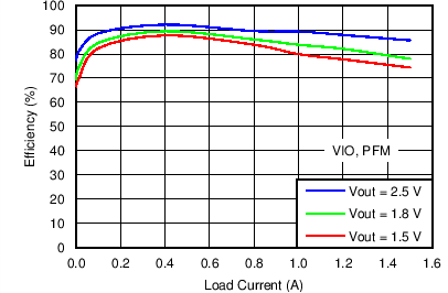 Figure 26. VIO Efficiency vs Load Current,
 25°C VIN = 4 V, PFM
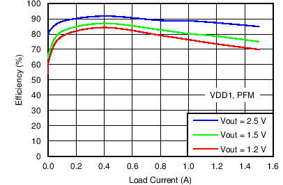 Figure 28. VDD1 Efficiency vs Load Current,
 25°C, VIN = 4 V, PFM
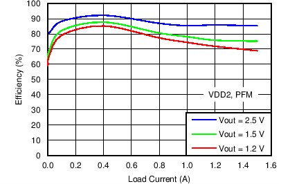 Figure 30. VDD2 Efficiency vs Load Current,
 25°C, VIN = 4 V, PFM
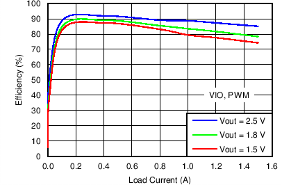 Figure 27. VIO Efficiency vs Load Current,
 25°C, VOUT = 2.5 V, VIN = 4 V, PWM
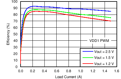 Figure 29. VDD1 Efficiency vs Load Current,
 25°C, VIN = 4 V, PWM
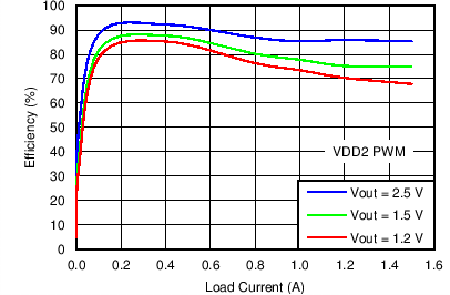 Figure 31. VDD2 Efficiency vs Load Current,
 25°C, VIN = 4 V, PWM
