SWCS032F October 2008 – July 2014 TPS65950
PRODUCTION DATA.
- 1Device Overview
- 2Revision History
- 3Terminal Configuration and Functions
- 4Specifications
-
5Detailed Description
- 5.1
Power Module
- 5.1.1
Power Providers
- 5.1.1.1 VDD1 DC-DC Regulator
- 5.1.1.2 VDD2 DC-DC Regulator
- 5.1.1.3 VIO DC-DC Regulator
- 5.1.1.4 VDAC LDO Regulator
- 5.1.1.5 VPLL1 LDO Regulator
- 5.1.1.6 VPLL2 LDO Regulator
- 5.1.1.7 VMMC1 LDO Regulator
- 5.1.1.8 VMMC2 LDO Regulator
- 5.1.1.9 VSIM LDO Regulator
- 5.1.1.10 VAUX1 LDO Regulator
- 5.1.1.11 VAUX2 LDO Regulator
- 5.1.1.12 VAUX3 LDO Regulator
- 5.1.1.13 VAUX4 LDO Regulator
- 5.1.1.14 Internal LDOs
- 5.1.1.15 CP
- 5.1.1.16 USB LDO Short-Circuit Protection Scheme
- 5.1.2 Power References
- 5.1.3 Power Control
- 5.1.4 Power Consumption
- 5.1.5 Power Management
- 5.1.1
Power Providers
- 5.2 Real-Time Clock and Embedded Power Controller
- 5.3
Audio/Voice Module
- 5.3.1 Audio/Voice Downlink (RX) Module
- 5.3.2
Audio/Voice Uplink (TX) Module
- 5.3.2.1 Microphone Bias Module
- 5.3.2.2 Stereo Differential Input
- 5.3.2.3 Headset Differential Input
- 5.3.2.4 FM Radio/Auxiliary Stereo Input
- 5.3.2.5 PDM Interface for Digital Microphones
- 5.3.2.6 Uplink Characteristics
- 5.3.2.7 Microphone Amplification Stage
- 5.3.2.8 Carkit Input
- 5.3.2.9 Digital Audio Filter Module
- 5.3.2.10 Digital Voice Filter Module
- 5.4
USB HS 2.0 OTG Transceiver
- 5.4.1 USB Features
- 5.4.2
USB Transceiver
- 5.4.2.1 MCPC Carkit Port Timing
- 5.4.2.2 USB-CEA Carkit Port Timing
- 5.4.2.3 HS USB Port Timing
- 5.4.2.4
PHY Electrical Characteristics
- 5.4.2.4.1 5-V Tolerance
- 5.4.2.4.2 LS/FS Single-Ended Receivers
- 5.4.2.4.3 LS/FS Differential Receiver
- 5.4.2.4.4 LS/FS Differential Transmitter
- 5.4.2.4.5 HS Differential Receiver
- 5.4.2.4.6 HS Differential Transmitter
- 5.4.2.4.7 CEA/MCPC/UART Driver
- 5.4.2.4.8 Pullup/Pulldown Resistors
- 5.4.2.4.9 PHY DPLL Electrical Characteristics
- 5.4.2.4.10 PHY Power Consumption
- 5.4.2.5 OTG Electrical Characteristics
- 5.5 Battery Interface
- 5.6 MADC
- 5.7 LED Drivers
- 5.8 Keyboard
- 5.9 Clock Specifications
- 5.10 Debouncing Time
- 5.11 External Components
- 5.1
Power Module
- 6Device and Documentation Support
Package Options
Refer to the PDF data sheet for device specific package drawings
Mechanical Data (Package|Pins)
- ZXN|209
Thermal pad, mechanical data (Package|Pins)
Orderable Information
6 Device and Documentation Support
6.1 Device Support
6.1.1 Development Support
TI offers an extensive line of development tools, including tools to evaluate the performance of the processors, generate code, develop algorithm implementations, and fully integrate and debug software and hardware modules. The tool's support documentation is electronically available within the Code Composer Studio™ Integrated Development Environment (IDE).
The following products support development of the TPS65950 device applications:
Software Development Tools: Code Composer Studio™ Integrated Development Environment (IDE): including Editor C/C++/Assembly Code Generation, and Debug plus additional development tools Scalable, Real-Time Foundation Software (DSP/BIOS™), which provides the basic run-time target software needed to support any TPS65950 device application.
Hardware Development Tools: Extended Development System (XDS™) Emulator
6.1.2 Device Nomenclature
To designate the stages in the product development cycle, TI assigns prefixes to the part numbers of all microprocessors (MPUs) and support tools. Each device has one of three prefixes: X, P, or null (no prefix) (for example, TPS65950). Texas Instruments recommends two of three possible prefix designators for its support tools: TMDX and TMDS. These prefixes represent evolutionary stages of product development from engineering prototypes (TMDX) through fully qualified production devices and tools (TMDS).
Device development evolutionary flow:
-
PPrototype (X), preproduction (P), or qualified/production device (blank). A blank in the symbol or part number is collapsed so there are no gaps between characters.
-
A Mask set version descriptor (initial silicon = blank, first silicon revision = A, second silicon revision = B, ...). Initial silicon version is ES1.0; first revision can be named ES2.0, ES1.1, or ES1.01, depending on the level of change. Note: Device name is a maximum of 10 characters.
-
YMYear month
-
LLLLSLot code
-
$Fab planning code
"Developmental product is intended for internal evaluation purposes."
Production devices and TMDS development-support tools have been characterized fully, and the quality and reliability of the device have been demonstrated fully. TI's standard warranty applies.
Predictions show that prototype devices (X or P) have a greater failure rate than the standard production devices. Texas Instruments recommends that these devices not be used in any production system because their expected end-use failure rate still is undefined. Only qualified production devices are to be used.
TI device nomenclature also includes a suffix with the device family name. This suffix indicates the package type (for example, ZXN) and the temperature range (for example, blank is the default commercial temperature range).
For orderable part numbers of TPS65950 devices in the ZXN package types, see the Package Option Addendum of this document, the TI website (www.ti.com), or contact your TI sales representative.
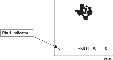 Figure 6-1 Device Nomenclature
6.2 Documentation Support
The following documents describe the TPS65950 device. Copies of these documents are available on the Internet at www.ti.com.
6.3 Community Resources
The following links connect to TI community resources. Linked contents are provided "AS IS" by the respective contributors. They do not constitute TI specifications and do not necessarily reflect TI's views; see TI's Terms of Use.
-
TI E2E™ Online Community TI's Engineer-to-Engineer (E2E) Community. Created to foster collaboration among engineers. At e2e.ti.com, you can ask questions, share knowledge, explore ideas and help solve problems with fellow engineers.
-
TI Embedded Processors Wiki Texas Instruments Embedded Processors Wiki. Established to help developers get started with Embedded Processors from Texas Instruments and to foster innovation and growth of general knowledge about the hardware and software surrounding these devices.
6.4 Trademarks
SmartReflex, OMAP, E2E are trademarks of Texas Instruments.
Bluetooth is a registered trademark of Bluetooth SIG, Inc.
6.5 Electrostatic Discharge Caution

This integrated circuit can be damaged by ESD. Texas Instruments recommends that all integrated circuits be handled with appropriate precautions. Failure to observe proper handling and installation procedures can cause damage.
ESD damage can range from subtle performance degradation to complete device failure. Precision integrated circuits may be more susceptible to damage because very small parametric changes could cause the device not to meet its published specifications.
6.6 Export Control Notice
Recipient agrees to not knowingly export or re-export, directly or indirectly, any product or technical data (as defined by the U.S., EU, and other Export Administration Regulations) including software, or any controlled product restricted by other applicable national regulations, received from Disclosing party under this Agreement, or any direct product of such technology, to any destination to which such export or re-export is restricted or prohibited by U.S. or other applicable laws, without obtaining prior authorization from U.S. Department of Commerce and other competent Government authorities to the extent required by those laws.
6.7 Glossary
SLYZ022 — TI Glossary.
This glossary lists and explains terms, acronyms, and definitions.
6.8 Additional Acronyms
Additional acronyms used in this data sheet are described below.
| ADC | Analog-to-digital converter |
| ALC | Automatic level control |
| ARIB | Association of Radio Industries and Businesses |
| ASIC | Application-specific integrated circuit |
| BCI | Battery charger interface |
| BGA | Ball grid array |
| BT | Bluetooth |
| BW | Signal bandwidth |
| CMOS | Complementary metal oxide semiconductor |
| Codec | Coder/decoder |
| CMT | Cellular mobile telephone |
| CPU | Central processing unit |
| DAC | Digital-to-analog converter |
| DBB | Digital baseband |
| DCR | Direct current (dc) resistance |
| DM | Data manual |
| DSP | Digital signal processor |
| DVFS | Dynamic voltage and frequency scaling |
| ESD | Electrostatic discharge |
| ESR | Equivalent series resistance |
| FET | Field effect transistor |
| FSR | Full-scale range |
| GP | General-purpose |
| GPIO | General-purpose input/output |
| hiZ | High impedance |
| HS | High speed or high security |
| HW | Hardware |
| I2C | Inter-integrated circuit |
| I2S | Inter-IC sound |
| IC | Integrated circuit |
| ICN | Idle channel noise |
| ID | Identification |
| IDDQ | Direct drain quiescent current |
| IF | Interface |
| IO or I/O | Input/output |
| JTAG | Joint Test Action Group, IEEE 1149.1 standard |
| LED | Light emitting diode |
| LDO | Low-dropout regulator |
| LJF | Left-justified format |
| LS | Low speed |
| MADC | Monitoring analog-to-digital converter |
| MCPC | Mobile Computing Promotion Consortium |
| MEMS | Micro-electrical-mechanical system |
| NA, N/A | Not applicable |
| NRZI | Nonreturn to zero inverted |
| OCP | Open-core protocol |
| OTG | On-the-go |
| PBGA | Plastic ball grid array |
| PCB | Printed circuit board |
| PCM | Pulse-code modulation |
| PD | Pulldown |
| PDM | Pulse density modulated |
| PFM | Pulse frequency modulation |
| PLL | Phase-locked loop |
| PMOS | Portable media operating system |
| POL | Polarity |
| POR | Power-on reset |
| PSRR | Power supply ripple rejection |
| PU | Pullup |
| PWL | Pulse-width length |
| PWT | Pulse-width time |
| PWM | Pulse-width modulation |
| RFID | Radio frequency identification |
| RJF | Right-justified format |
| RTC | Real-time clock |
| RX | Receive |
| SDI | Serial display Interface |
| SMPS | Switch-mode power supply |
| SNR | Signal-to-noise ratio |
| SRP | Secure remote password |
| SW | Software |
| SYNC/SYNCHRO | Synchronization |
| SYS | System |
| TAP | Test access port |
| TBD | To be defined |
| TDM | Time division multiplexing |
| THRU | Feed through |
| TRM | Technical reference manual |
| TX | Transmit |
| UART | Universal asynchronous receiver/transmitter |
| ULPI | UTMI+ low pin interface |
| UPR | Uninterrupted power rail |
| USB | Universal serial bus |
| UTMI | USB transceiver macrocell interface |