SWCS032F October 2008 – July 2014 TPS65950
PRODUCTION DATA.
- 1Device Overview
- 2Revision History
- 3Terminal Configuration and Functions
- 4Specifications
-
5Detailed Description
- 5.1
Power Module
- 5.1.1
Power Providers
- 5.1.1.1 VDD1 DC-DC Regulator
- 5.1.1.2 VDD2 DC-DC Regulator
- 5.1.1.3 VIO DC-DC Regulator
- 5.1.1.4 VDAC LDO Regulator
- 5.1.1.5 VPLL1 LDO Regulator
- 5.1.1.6 VPLL2 LDO Regulator
- 5.1.1.7 VMMC1 LDO Regulator
- 5.1.1.8 VMMC2 LDO Regulator
- 5.1.1.9 VSIM LDO Regulator
- 5.1.1.10 VAUX1 LDO Regulator
- 5.1.1.11 VAUX2 LDO Regulator
- 5.1.1.12 VAUX3 LDO Regulator
- 5.1.1.13 VAUX4 LDO Regulator
- 5.1.1.14 Internal LDOs
- 5.1.1.15 CP
- 5.1.1.16 USB LDO Short-Circuit Protection Scheme
- 5.1.2 Power References
- 5.1.3 Power Control
- 5.1.4 Power Consumption
- 5.1.5 Power Management
- 5.1.1
Power Providers
- 5.2 Real-Time Clock and Embedded Power Controller
- 5.3
Audio/Voice Module
- 5.3.1 Audio/Voice Downlink (RX) Module
- 5.3.2
Audio/Voice Uplink (TX) Module
- 5.3.2.1 Microphone Bias Module
- 5.3.2.2 Stereo Differential Input
- 5.3.2.3 Headset Differential Input
- 5.3.2.4 FM Radio/Auxiliary Stereo Input
- 5.3.2.5 PDM Interface for Digital Microphones
- 5.3.2.6 Uplink Characteristics
- 5.3.2.7 Microphone Amplification Stage
- 5.3.2.8 Carkit Input
- 5.3.2.9 Digital Audio Filter Module
- 5.3.2.10 Digital Voice Filter Module
- 5.4
USB HS 2.0 OTG Transceiver
- 5.4.1 USB Features
- 5.4.2
USB Transceiver
- 5.4.2.1 MCPC Carkit Port Timing
- 5.4.2.2 USB-CEA Carkit Port Timing
- 5.4.2.3 HS USB Port Timing
- 5.4.2.4
PHY Electrical Characteristics
- 5.4.2.4.1 5-V Tolerance
- 5.4.2.4.2 LS/FS Single-Ended Receivers
- 5.4.2.4.3 LS/FS Differential Receiver
- 5.4.2.4.4 LS/FS Differential Transmitter
- 5.4.2.4.5 HS Differential Receiver
- 5.4.2.4.6 HS Differential Transmitter
- 5.4.2.4.7 CEA/MCPC/UART Driver
- 5.4.2.4.8 Pullup/Pulldown Resistors
- 5.4.2.4.9 PHY DPLL Electrical Characteristics
- 5.4.2.4.10 PHY Power Consumption
- 5.4.2.5 OTG Electrical Characteristics
- 5.5 Battery Interface
- 5.6 MADC
- 5.7 LED Drivers
- 5.8 Keyboard
- 5.9 Clock Specifications
- 5.10 Debouncing Time
- 5.11 External Components
- 5.1
Power Module
- 6Device and Documentation Support
Package Options
Refer to the PDF data sheet for device specific package drawings
Mechanical Data (Package|Pins)
- ZXN|209
Thermal pad, mechanical data (Package|Pins)
Orderable Information
4 Specifications
4.1 Absolute Maximum Ratings
over operating free-air temperature range (unless otherwise noted)| Parameter | Test Conditions | Min | Typ | Max | Unit |
|---|---|---|---|---|---|
| Main battery supply voltage(1) | 2.1 | 4.5 | V | ||
| Voltage on any input | Where supply represents the voltage applied to the power supply pin associated with the input | 0.0 | 1.0*Supply | V | |
| Storage temperature range | –55 | 125 | °C | ||
| Ambient temperature range | –40 | 85 | °C | ||
| Junction temperature (TJ) | At 1.4W (Theta JB 11°C/W 2S2P board) | 105 | °C | ||
| Junction temperature (TJ) for parametric compliance | –40 | 105 | °C |
4.2 Handling Ratings
| MIN | MAX | UNIT | ||||
|---|---|---|---|---|---|---|
| Tstg | Storage temperature range | –45 | 150 | °C | ||
| VESD | Electrostatic discharge (ESD) performance: | Human Body Model (HBM), per ANSI/ESDA/JEDEC JS001(1) | Internal pins | –1 | 1 | kV |
| External pins(3) | –2 | 2 | ||||
| Charged Device Model (CDM), per JESD22-C101(2) |
All pins | –500 | 500 | V | ||
4.3 Recommended Operating Conditions
over operating free-air temperature range (unless otherwise noted)| Parameter | Min | Typ | Max | Unit |
|---|---|---|---|---|
| Main battery supply voltage | 2.7(1) | 3.6 | 4.5 | V |
| Backup battery supply voltage | 1.8 | 3.2 | 3.3 | V |
| Ambient temperature range | –40 | 85 | °C |
4.4 Digital I/O Electrical Characteristics(1)
| Pin Name | VOL (V) | VOH (V) | VIL (V) | VIH (V) | Max Freq (MHz) | Load (pF) Output Mode | Rise Time (ns) | Fall Time (ns) | ||||
|---|---|---|---|---|---|---|---|---|---|---|---|---|
| Min | Max | Min | Max | Min | Max | Min | Max | |||||
| GPIO0/CD1 | 0 | 0.45 | RL–0.45 | RL | 0 | 0.35xRL | 0.65xRL | RL | 33 | 30 | 5.2 | 5.2 |
| JTAG.TDO | ||||||||||||
| GPIO0/CD2 | 0 | 0.45 | RL–0.45 | RL | 0 | 0.35xRL | 0.65xRL | RL | 33 | 30 | 5.2 | 5.2 |
| JTAG.TMS | ||||||||||||
| GPIO2 | 0 | 0.45 | RL–0.45 | RL | 0 | 0.35xRL | 0.65xRL | RL | 3 | 30 | 5.2 | 5.2 |
| Test1 | ||||||||||||
| GPIO15 | 0 | 0.45 | RL–0.45 | RL | 0 | 0.35xRL | 0.65xRL | RL | 3 | 30 | 5.2 | 5.2 |
| Test2 | ||||||||||||
| GPIO16 | 0 | 0.45 | RL–0.45 | RL | 0 | 0.35xRL | 0.65xRL | RL | 3 | 30 | 5.2 | 5.2 |
| PWM0 | ||||||||||||
| Test3 | ||||||||||||
| GPIO17 | 0 | 0.45 | RL–0.45 | RL | 0 | 0.35xRL | 0.65xRL | RL | 3 | 30 | 5.2 | 5.2 |
| VIBRA.SYNC | ||||||||||||
| PWM1 | ||||||||||||
| Test4 | ||||||||||||
| START.ADC | 0 | 0.45 | RL–0.45 | RL | 0 | 0.35×RL | 0.65×RL | RL | 6 | 16.7 | 16.7 | |
| SYSEN | 0 | 0.45 | RL–0.45 | RL | 0 | 0.35×RL | 0.65×RL | RL | 5.2 | 5.2 | ||
| CLKEN | 0 | 0.45 | RL–0.45 | RL | 0 | 0.35×RL | 0.65×RL | RL | 3 | 30 | 33.3 | 33.3 |
| CLKEN2 | 0 | 0.45 | RL–0.45 | RL | 0 | 0.35×RL | 0.65×RL | RL | 3 | 30 | 33.3 | 33.3 |
| CLKREQ | 0 | 0.45 | RL–0.45 | RL | 0 | 0.35×RL | 0.65×RL | RL | 3 | 33.3 | 33.3 | |
| INT1 | 0 | 0.45 | RL–0.45 | RL | 0 | 0.35×RL | 0.65×RL | RL | 3 | 30 | 33.3 | 33.3 |
| INT2 | 0 | 0.45 | RL–0.45 | RL | 0 | 0.35×RL | 0.65×RL | RL | 3 | 30 | 33.3 | 33.3 |
| NRESPWRON | 0 | 0.45 | RL–0.45 | RL | 0 | 0.35×RL | 0.65×RL | RL | 3 | 30 | 33.3 | 33.3 |
| NRESWARM | 0 | 0.45 | RL–0.45 | RL | 0 | 0.35×RL | 0.65×RL | RL | 3 | 30 | 33.3 | 33.3 |
| PWRON | 0 | 0.35×1.8V | 0.65×1.8V | VBAT | 3 | 33.3 | 33.3 | |||||
| NSLEEP1 | 0 | 0.45 | RL–0.45 | RL | 0 | 0.35×RL | 0.65×RL | RL | 3 | 33.3 | 33.3 | |
| NSLEEP2 | 0 | 0.45 | RL–0.45 | RL | 0 | 0.35×RL | 0.65×RL | RL | 3 | 33.3 | 33.3 | |
| CLK256FS | 0 | 0.45 | RL–0.45 | RL | 0 | 0.35×RL | 0.65×RL | RL | 12.288 | 30 | 16.3 | 16.3 |
| VMODE1 | 0 | 0.45 | RL–0.45 | RL | 0 | 0.35×RL | 0.65×RL | RL | 3 | 33.3 | 33.3 | |
| BOOT0 | 0 | RL | 3 | 33.3 | 33.3 | |||||||
| BOOT1 | 0 | RL | 3 | 33.3 | 33.3 | |||||||
| REGEN | 0 | 0.45 | RL–0.45 | RL | 0 | 0.35×RL | 0.65×RL | RL | 3 | 30 | 33.3 | 33.3 |
| MSECURE | 0 | 0.45 | RL–0.45 | RL | 0 | 0.35×RL | 0.65×RL | RL | 3 | 33.3 | 33.3 | |
| I2C.SR.SDA | 0 | 0.4 | –0.5 | 0.3×RL | 0.7×RL | RL+0.5 | 3.4 | Up to 400 | ||||
| VMODE2 | 0 | 0.45 | RL–0.45 | RL | 0 | 0.35×RL | 0.65×RL | RL | 3.4 | 29.4 | 29.4 | |
| I2C.SR.SCL | 0 | 0.4 | –0.5 | 0.3×RL | 0.7×RL | RL+0.5 | 3.4 | 10.0 | 10.0 | |||
| I2C.CNTL.SDA | 0 | 0.4 | –0.5 | 0.3×RL | 0.7×RL | RL+0.5 | 3.4 | Up to 400 | ||||
| I2C.CNTL.SCL | 0 | 0.4 | –0.5 | 0.3×RL | 0.7×RL | RL+0.5 | 3.4 | 10.0 | 10.0 | |||
| PCM.VCK | 0 | 0.45 | RL–0.45 | RL | 0 | 0.35×RL | 0.65×RL | RL | 1 | 30 | 100.0 | 33.0 |
| PCM.VDR | 0 | 0.45 | RL–0.45 | RL | 0 | 0.35×RL | 0.65×RL | RL | 1 | 30 | 100.0 | 100.0 |
| PCM.VDX | 0 | 0.45 | RL–0.45 | RL | 0 | 0.35×RL | 0.65×RL | RL | 1 | 30 | 100.0 | 33.0 |
| PCM.VFS | 0 | 0.45 | RL–0.45 | RL | 0 | 0.35×RL | 0.65×RL | RL | 1 | 30 | 33.0 | 33.0 |
| I2S.CLK | 0 | 0.45 | RL–0.45 | RL | 0 | 0.35×RL | 0.65×RL | RL | 6.5 | 30 | 33.0 | 33.0 |
| I2S.SYNC | 0 | 0.45 | RL–0.45 | RL | 0 | 0.35×RL | 0.65×RL | RL | 6.5 | 30 | 33.0 | 33.0 |
| I2S.DIN | 0 | 0.45 | RL–0.45 | RL | 0 | 0.35×RL | 0.65×RL | RL | 3.25 | 30 | 33.0 | 33.0 |
| I2S.DOUT | 0 | 0.45 | RL–0.45 | RL | 0 | 0.35×RL | 0.65×RL | RL | 3.25 | 30 | 29.0 | 29.0 |
| UART1.TXD | 0 | 0.45 | RL–0.45 | RL | 0 | 0.35×RL | 0.65×RL | RL | 3 | 30 | 33.0 | 33.0 |
| GPIO8 | 0 | 0.45 | RL–0.45 | RL | 0 | 0.35×RL | 0.65×RL | RL | 3 | 33.0 | 33.0 | |
| UART1.RXD | ||||||||||||
| RTSO/CLD64K.OUT/ BERCLK.OUT |
0 | 0.45 | RL–0.45 | RL | 0 | 0.35×RL | 0.65×RL | RL | 3 | 30 | 33.0 | 33.0 |
| CTSI/BERDATA.OUT | 0 | 0.45 | RL–0.45 | RL | 0 | 0.35×RL | 0.65×RL | RL | 3 | 30 | 33.0 | 33.0 |
| MANU | 0 | 0.45 | RL–0.45 | RL | 0 | 0.35×RL | 0.65×RL | RL | 3 | 33.0 | 33.0 | |
| 32KCLKOUT | 0 | 0.45 | RL–0.45 | RL | 0 | 0.35×RL | 0.65×RL | RL | 0.032 | 30 | 16 | 16 |
| HFCLKOUT | 0 | 0.45 | RL–0.45 | RL | 0 | 0.35×RL | 0.65×RL | RL | 38.4 | 30 | 2.6 | 2.6 |
| UCLK | 0 | 0.45 | RL–0.45 | RL | 0 | 0.35×RL | 0.65×RL | RL | 60 | 10 | 1.0 | 1.0 |
| STP | 0 | 0.45 | RL–0.45 | RL | 0 | 0.35×RL | 0.65×RL | RL | 30 | 10 | 1.0 | 1.0 |
| GPIO9 | ||||||||||||
| DIR | 0 | 0.45 | RL–0.45 | RL | 0 | 0.35×RL | 0.65×RL | RL | 30 | 10 | 1.0 | 1.0 |
| GPIO10 | ||||||||||||
| NXT | 0 | 0.45 | RL–0.45 | RL | 0 | 0.35×RL | 0.65×RL | RL | 30 | 10 | 1.0 | 1.0 |
| GPIO11 | ||||||||||||
| DATA0 | 0 | 0.45 | RL–0.45 | RL | 0 | 0.35×RL | 0.65×RL | RL | 30 | 10 | 1.0 | 1.0 |
| UART4.TXD | ||||||||||||
| DATA1 | 0 | 0.45 | RL–0.45 | RL | 0 | 0.35×RL | 0.65×RL | RL | 30 | 10 | 1.0 | 1.0 |
| UART4.RXD | ||||||||||||
| DATA2 | 0 | 0.45 | RL–0.45 | RL | 0 | 0.35×RL | 0.65×RL | RL | 30 | 10 | 1.0 | 1.0 |
| UART4.RTSI | ||||||||||||
| DATA3 | 0 | 0.45 | RL–0.45 | RL | 0 | 0.35×RL | 0.65×RL | RL | 30 | 10 | 1.0 | 1.0 |
| UART4.CTSO | ||||||||||||
| GPIO12 | 0 | 0.45 | RL–0.45 | RL | 0 | 0.35×RL | 0.65×RL | RL | 30 | 10 | 1.0 | 1.0 |
| DATA4 | 0 | 0.45 | RL–0.45 | RL | 0 | 0.35×RL | 0.65×RL | RL | 30 | 10 | 1.0 | 1.0 |
| GPIO14 | ||||||||||||
| DATA5 | 0 | 0.45 | RL–0.45 | RL | 0 | 0.35×RL | 0.65×RL | RL | 30 | 10 | 1.0 | 1.0 |
| GPIO3 | ||||||||||||
| DATA6 | 0 | 0.45 | RL–0.45 | RL | 0 | 0.35×RL | 0.65×RL | RL | 30 | 10 | 1.0 | 1.0 |
| GPIO4 | ||||||||||||
| DATA7 | 0 | 0.45 | RL–0.45 | RL | 0 | 0.35×RL | 0.65×RL | RL | 30 | 10 | 1.0 | 1.0 |
| GPIO5 | ||||||||||||
| Test.RESET | 0 | 0.45 | RL–0.45 | RL | 0 | 0.35×RL | 0.65×RL | RL | 3 | 33.0 | 33.0 | |
| Test | 0 | 0.45 | RL–0.45 | RL | 0 | 0.35×RL | 0.65×RL | RL | 3 | 30 | 29.0 | 29.0 |
| JTAG.TDI/ BERDATA | 0 | 0.45 | RL–0.45 | RL | 0 | 0.35×RL | 0.65×RL | RL | 3 | 33.0 | 33.0 | |
| JTAG.TCK/ BERDATA | 0 | 0.45 | RL–0.45 | RL | 0 | 0.35×RL | 0.65×RL | RL | 3 | 33.0 | 33.0 | |
| GPIO13 | 0 | 0.45 | RL–0.45 | RL | 0 | 0.35×RL | 0.35×RL | 3 | 30 | 33.3 | 33.3 | |
| LEDSYNC | ||||||||||||
| KPD.C0 | 0 | 0.45 | RL–0.45 | RL | 0 | 0.35×RL | 0.65×RL | RL | 0.033 | 30 | 29.0 | 29.0 |
| KPD.C1 | 0 | 0.45 | RL–0.45 | RL | 0 | 0.35×RL | 0.65×RL | RL | 0.033 | 30 | 29.0 | 29.0 |
| KPD.C2 | 0 | 0.45 | RL–0.45 | RL | 0 | 0.35×RL | 0.65×RL | RL | 0.033 | 30 | 29.0 | 29.0 |
| KPD.C3 | 0 | 0.45 | RL–0.45 | RL | 0 | 0.35×RL | 0.65×RL | RL | 0.033 | 30 | 29.0 | 29.0 |
| KPD.C4 | 0 | 0.45 | RL–0.45 | RL | 0 | 0.35×RL | 0.65×RL | RL | 0.033 | 30 | 29.0 | 29.0 |
| KPD.C5 | 0 | 0.45 | RL–0.45 | RL | 0 | 0.35×RL | 0.65×RL | RL | 0.033 | 30 | 29.0 | 29.0 |
| KPD.C6 | 0 | 0.45 | RL–0.45 | RL | 0 | 0.35×RL | 0.65×RL | RL | 0.033 | 30 | 29.0 | 29.0 |
| KPD.C7 | 0 | 0.45 | RL–0.45 | RL | 0 | 0.35×RL | 0.65×RL | RL | 0.033 | 30 | 29.0 | 29.0 |
| KPD.R0 | 0 | 0.45 | RL–0.45 | RL | 0 | 0.35×RL | 0.65×RL | RL | 0.033 | 3051.8 | 3051.8 | |
| KPD.R1 | 0 | 0.45 | RL–0.45 | RL | 0 | 0.35×RL | 0.65×RL | RL | 0.033 | 3051.8 | 3051.8 | |
| KPD.R2 | 0 | 0.45 | RL–0.45 | RL | 0 | 0.35×RL | 0.65×RL | RL | 0.033 | 3051.8 | 3051.8 | |
| KPD.R3 | 0 | 0.45 | RL–0.45 | RL | 0 | 0.35×RL | 0.65×RL | RL | 0.033 | 3051.8 | 3051.8 | |
| KPD.R4 | 0 | 0.45 | RL–0.45 | RL | 0 | 0.35×RL | 0.65×RL | RL | 0.033 | 3051.8 | 3051.8 | |
| KPD.R5 | 0 | 0.45 | RL–0.45 | RL | 0 | 0.35×RL | 0.65×RL | RL | 0.033 | 3051.8 | 3051.8 | |
| KPD.R6 | 0 | 0.45 | RL–0.45 | RL | 0 | 0.35×RL | 0.65×RL | RL | 0.033 | 3051.8 | 3051.8 | |
| KPD.R7 | 0 | 0.45 | RL–0.45 | RL | 0 | 0.35×RL | 0.65×RL | RL | 0.033 | 3051.8 | 3051.8 | |
| GPIO16 | 0 | 0.45 | RL–0.45 | RL | 0 | 0.35×RL | 0.65×RL | RL | 3 | 30 | 33.3 | 33.3 |
| DIG.MIC.CLK0 | 0 | 0.45 | RL–0.45 | RL | 0 | 0.35×RL | 0.65×RL | RL | 2.4 | 30 | 41.7 | 41.7 |
| BT.PCM.VDX | 0 | 0.45 | RL–0.45 | RL | 0 | 0.35×RL | 0.65×RL | RL | 1 | 30 | 100.0 | 100.0 |
| GPIO17 | 0 | 0.45 | RL–0.45 | RL | 0 | 0.35×RL | 0.65×RL | RL | 3 | 30 | 33.3 | 33.3 |
| DIG.MIC.CLK1 | 0 | 0.45 | RL–0.45 | RL | 0 | 0.35×RL | 0.65×RL | RL | 2.4 | 30 | 41.7 | 41.7 |
| BT.PCM.VDX | 0 | 0.45 | RL–0.45 | RL | 0 | 0.35×RL | 0.65×RL | RL | 1 | 30 | 100.0 | 100.0 |
| RFID.EN | ||||||||||||
- RL: Reference level voltage applied to the I/O cell
- VOL: Low-level output voltage
- VOH: High-level output voltage
- VIL: Low-level input voltage
- VIH: High-level input voltage
4.5 Thermal Resistance Characteristics for ZXN Package
| NAME | DESCRIPTION | °C/W(1)(2) | AIR FLOW (m/s)(3) |
|---|---|---|---|
| RΘJC | Junction-to-case (top) | 12.9 | 0.00 |
| RΘJB | Junction-to-board | 11.2 | 0.00 |
| RΘJA
(High k PCB) |
Junction-to-free air | 37.6 | 0.00 |
| PsiJT | Junction-to-package top | 0.2 | 0.00 |
| PsiJB | Junction-to-board | 9.5 | 0.00 |
- JESD51-2, Integrated Circuits Thermal Test Method Environmental Conditions - Natural Convection (Still Air)
- JESD51-3, Low Effective Thermal Conductivity Test Board for Leaded Surface Mount Packages
- JESD51-7, High Effective Thermal Conductivity Test Board for Leaded Surface Mount Packages
- JESD51-9, Test Boards for Area Array Surface Mount Package Thermal Measurements
4.6 Minimum Voltages and Associated Currents
| Category | Pin and Module | Maximum Current Specified (mA) | Output Voltage (V) | VBAT Minimum (V) |
|---|---|---|---|---|
| VBAT pin name | VDD_VPLLA3R_IN_6POV | 340 | ||
| Internal module supplied | VPLL1 (LDO) | 40 | 1.0 / 1.2 / 1.3 / 1.8 / 2.8 / 3.0 | Maximum (2.7, output voltage selected + 250 mV) |
| VPLL2 (LDO) | 100 | 0.7 / 1.0 / 1.2 / 1.3 / 1.5 / 1.8 / 1.85 / 2.5 / 2.6 / 2.8 / 2.85 / 3.0 / 3.15 | Maximum (2.7, output voltage selected + 250 mV) |
|
| VAUX3 (LDO) | 200 | 1.5 / 1.8 / 2.5 / 2.8 / 3.0 | Maximum (2.7, output voltage selected + 250 mV) |
|
| VDD1 core (DCDC) | < 1 | 2.7 | ||
| VDD2 core (DCDC) | < 1 | 2.7 | ||
| SYSPOR (power ref) | < 1 | 2.7 | ||
| PBIAS (power ref) | < 1 | 2.7 | ||
| VBAT pin name | VDD_VDAC_IN_6POV | 370 | ||
| Internal module supplied | VDAC (LDO) | 70 | 1.2 / 1.3 / 1.8 | Maximum (2.7, output voltage selected + 250 mV) |
| VINTANA1 (LDO) | 50 | 1.5 | Maximum (2.7, output voltage selected + 250 mV) |
|
| VINTANA2 (LDO) | 250 | 2.5 / 2.75 | Maximum (2.7, output voltage selected +250 mV) |
|
| VIO core (DCDC) | < 1 | 2.7 | ||
| VAUX4 core (LDO) | < 1 | 2.7 | ||
| VBAT pin name | VDD_VAUXI2S_IN_6POV | 350 | ||
| Internal module supplied | VAUX1 (LDO) | 200 | 1.5 / 1.8 / 2.5 / 2.8 / 3.0 | Maximum (2.7, output voltage selected + 250 mV) |
| VAUX2 (LDO) | 100 | 1.3 / 1.5 / 1.6 / 1.7 / 1.8 / 1.9 / 2.0 / 2.1 / 2.2 / 2.3 / 2.4 / 2.5 / 2.8 | Maximum (2.7, output voltage selected + 250 mV) |
|
| VSIM (LDO) | 50 | 1.0 / 1.2 / 1.3 / 1.8 / 2.8 / 3.0 | Maximum (2.7, output voltage selected + 250 mV) |
|
| VBAT pin name | VDD_VMMC2_IN_6POV | 100 | ||
| VMMC2 (LDO) | 100 | 1.0 / 1.2 / 1.3 / 1.5 / 1.8 / 1.85 / 2.5 / 2.6 / 2.8 / 2.85 / 3.0 / 3.15 | Maximum (2.7, output voltage selected + 250 mV) |
|
| Power_REGBATT | 0.001 | 2.7 | ||
| VBAT pin name | VDD_VMMC1_IN_6POV | 220 | ||
| VMMC1 (LDO) | 220 | 1.85 / 2.85 / 3.0 / 3.15 | Maximum (2.7, output voltage selected + 250 mV) |
|
| Power_REGBATT | 0.001 | 2.7 | ||
| VBAT pin name | VDD_VINT_IN_6POV | 131 | ||
| Internal module supplied | VINTDIG (LDO) | 80 | 1.0 / 1.2 / 1.3 / 1.5 | Maximum (2.7, output voltage selected + 250 mV) |
| VRRTC (LDO) | 30 | 1.5 | Maximum (2.7, output voltage selected + 250 mV) |
|
| VBACKUP (LDO) | 1 | 2.5 / 3.0 / 3.1 / 3.2 | Maximum (2.7, output voltage selected + 250 mV) |
|
| VBAT pin name | VDD_VAUX4_IN_6POV | 100 | ||
| VAUX4 (LDO) | 100 | 0.7 / 1.0 / 1.2 / 1.3 / 1.5 / 1.8 / 1.85 / 2.5 / 2.6 / 2.8 / 2.85 / 3.0 / 3.15 | output voltage selected + 250 mV |
4.7 Timing Requirements and Switching Characteristics
4.7.1 Timing Parameters
The timing parameter symbols used in the timing requirement and switching characteristic tables are created in accordance with JEDEC Standard 100. To shorten the symbols, some pin names and other related terminologies are abbreviated as shown in Table 4-1.
Table 4-1 Timing Parameters
| Lowercase Subscripts | |
|---|---|
| Symbol | Parameter |
| c | Cycle time (period) |
| d | Delay time |
| dis | Disable time |
| en | Enable time |
| h | Hold time |
| su | Setup time |
| START | Start-bit |
| t | Transition time |
| v | Valid time |
| w | Pulse duration (width) |
| X | Unknown, changing, or don't care level |
| H | High |
| L | Low |
| V | Valid |
| IV | Invalid |
| AE | Active edge |
| FE | First edge |
| LE | Last edge |
| Z | High impedance |
4.7.2 Target Frequencies
Table 4-2 assumes testing over the recommended operating conditions.
Table 4-2 TPS65950 Interface Target Frequencies
| I/O Interface | Interface Designation | Target Frequency | |
|---|---|---|---|
| 1.5 V | |||
| SmartReflex I2C | I2C interface | Slave HS mode | 3.6 Mbps |
| GP I2C | Slave fast-speed mode | 400 kbps | |
| Slave standard mode | 100 kbps | ||
| USB | USB | HS | 480 Mbps |
| FS | 12 Mbps | ||
| LS | 1.5 Mbps | ||
| JTAG | RealView® ICE tool | 30 MHz | |
| XDS560 and XDS510 tools | 30 MHz | ||
| Lauterbach™ tool | 30 MHz | ||
| TDM/I2S | Inter-IC sound (I2S™) | 1/(64 * Fs)(1) | |
| Right-justified | 1/(64 * Fs)(1) | ||
| Left-justified | 1/(64 * Fs)(1) | ||
| TDM | 1/(128 * Fs)(1) | ||
| Voice/Bluetooth PCM interface | PCM (master mode) | 1/(65 * Fs)(2) | |
| PCM (slave mode) | 1/(33 to 65 * Fs)(2) | ||
4.7.3 I2C Timing
The TPS65950 provides two I2C HS slave interfaces (one for GP and one for SmartReflex). These interfaces support the standard mode (100 kbps), fast mode (400 kbps), and HS mode (3.4 Mbps). The GP I2C module embeds four slave hard-coded addresses (ID1 = 48h, ID2 = 49h, ID3 = 4Ah, and ID4 = 4Bh). The SmartReflex I2C module uses one slave hard-coded address (ID5). Master mode is not supported.
Table 4-3 and Table 4-4 assume testing over the recommended operating conditions (see Figure 4-1).
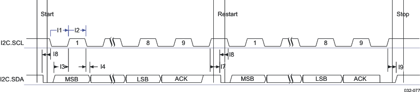 Figure 4-1 I2C Interface—Transmit and Receive in Slave Mode
Table 4-3 I2C Interface Timing Requirements(1)(2)
| Notation | Parameter | Min | Max | Unit | |
|---|---|---|---|---|---|
| Slave HS Mode | |||||
| I3 | tsu(SDA-SCLH) | Setup time, SDA valid to SCL high | 10 | ns | |
| I4 | th(SCLL-SDA) | Hold time, SDA valid from SCL low | 0 | 70 | ns |
| I7 | tsu(SCLH-SDAL) | Setup time, SCL high to SDA low | 160 | ns | |
| I8 | th(SDAL-SCLL) | Hold time, SCL low from SDA low | 160 | ns | |
| I9 | tsu(SDAH-SCLH) | Setup time, SDA high to SCL high | 160 | ns | |
| Slave Fast-Speed Mode | |||||
| I3 | tsu(SDA-SCLH) | Setup time, SDA valid to SCL high | 100 | ns | |
| I4 | th(SCLL-SDA) | Hold time, SDA valid from SCL low | 0 | 0.9 | ns |
| I7 | tsu(SCLH-SDAL) | Setup time, SCL high to SDA low | 0.6 | ns | |
| I8 | th(SDAL-SCLL) | Hold time, SCL low from SDA low | 0.6 | ns | |
| I9 | tsu(SDAH-SCLH) | Setup time, SDA high to SCL high | 0.6 | ns | |
| Slave Standard Mode | |||||
| I3 | tsu(SDA-SCLH) | Setup time, SDA valid to SCL high | 250 | ns | |
| I4 | th(SCLL-SDA) | Hold time, SDA valid from SCL low | 0 | ns | |
| I7 | tsu(SCLH-SDAL) | Setup time, SCL high to SDA low | 4.7 | ns | |
| I8 | th(SDAL-SCLL) | Hold time, SCL low from SDA low | 4 | ns | |
| I9 | tsu(SDAH-SCLH) | Setup time, SDA high to SCL high | 4 | ns | |
80 ns in HS mode (3.4 Mbps)
300 ns in fast-speed mode (400 Kbps)
1000 ns in standard mode (100 Kbps)
SCL equals I2C.SR.SCL or I2C.CNTL.SCL
Table 4-4 I2C Interface Switching Requirements(1)(2)
| Notation | Parameter | Min | Max | Unit | |
|---|---|---|---|---|---|
| Slave HS Mode | |||||
| I1 | tw(SCLL) | Pulse duration, SCL low | 160 | ns | |
| I2 | tw(SCLH) | Pulse duration, SCL high | 60 | ns | |
| Slave Fast-Speed Mode | |||||
| I1 | tw(SCLL) | Pulse duration, SCL low | 1.3 (3) | µs | |
| I2 | tw(SCLH) | Pulse duration, SCL high | 0.6 | µs | |
| Slave Standard Mode | |||||
| I1 | tw(SCLL) | Pulse duration, SCL low | 4.7 | µs | |
| I2 | tw(SCLH) | Pulse duration, SCL high | 4 | µs | |
100 pF in HS mode (3.4 Mbps)
400 pF in fast-speed mode (400 Kbps)
400 pF in standard mode (100 Kbps)
SCL equals I2C.SR.SCL or I2C.CNTL.SCL
4.7.4 Audio Interface: TDM/I2S Protocol
The TPS65950 acts as a master for the TDM and I2S interface or as a slave only for the I2S interface. If the TPS65950 is the master, it must provide frame synchronization (TDM/I2S_SYNC) and bit clock (TDM/I2S_CLK) to the host processor. If the TPS65950 is the slave, it receives frame synchronization and bit clock.
The TPS65950 supports the I2S, TDM, left-justified, and right-justified data formats, but does not support TDM slave mode.
4.7.4.1 I2S Right- and Left-Justified Data Format
Table 4-5 and Table 4-6 assume testing over the recommended operating conditions (see Figure 4-2 and Figure 4-3).
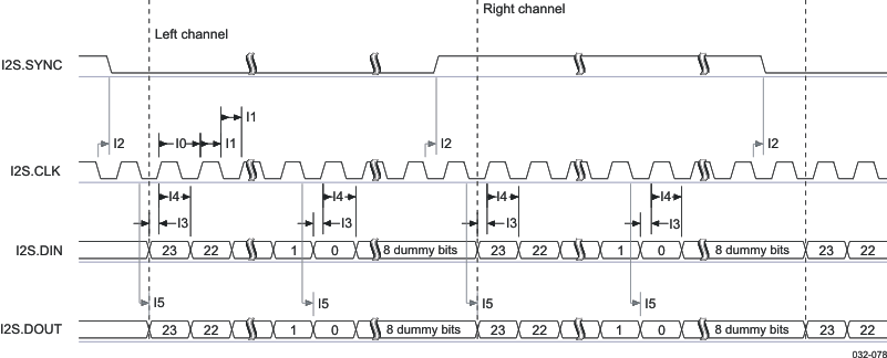 Figure 4-2 I2S Interface—I2S Master Mode
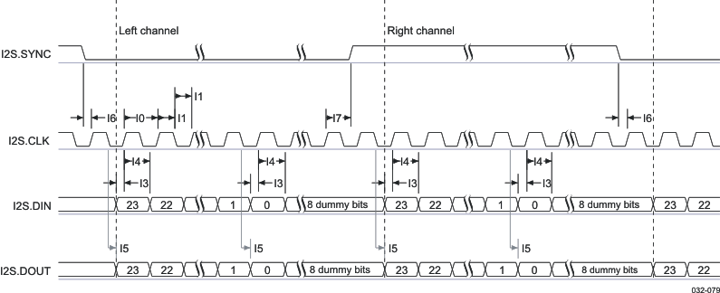 Figure 4-3 I2S Interface—I2S Slave Mode
The timing requirements in Table 4-5 are valid on the following conditions of input slew and output load:
- Rise and fall time range of inputs (SYNC, DIN) is tR/tF = 1.0 ns/6.5 ns
- Capacitance load range of outputs (CLK, SYNC, DOUT) is CLoad = 1 pF/30 pF
The input timing requirements in Table 4-5 are given by considering a rising or falling time of 6.5 ns.
Table 4-5 I2S Interface—Timing Requirements
| Notation | Parameter | Min | Max | Unit | |
|---|---|---|---|---|---|
| Master Mode | |||||
| I3 | tsu(DIN-CLKH) | Setup time, I2S.DIN valid to I2S.CLK high2 | 25 | ns | |
| I4 | th(DIN-CLKH) | Hold time, I2S.DIN valid from I2S.CLK high. | 0 | ns | |
| Slave Mode | |||||
| I0 | tc(CLK) | Cycle time, I2S.CLK(1) | 1/64 * Fs | ns | |
| I1 | tw(CLK) | Pulse duration, I2S.CLK high or low(2) | 0.45 * P | 0.55 * P | ns |
| I3 | tsu(DIN-CLKH) | Setup time, I2S.DIN valid to I2S.CLK high | 5 | ns | |
| I4 | th(DIN-CLKH) | Hold time, I2S.DIN valid from I2S.CLK high. | 5 | ns | |
| I6 | tsu(SYNC-CLKH) | Setup time, I2S.SYNC valid to I2S.CLK high | 5 | ns | |
| I7 | th(SYNC-CLKH) | Hold time, I2S.SYNC valid from I2S.CLK high | 5 | ns | |
The capacitive load for Table 4-6 is 7 pF.
Table 4-6 I2S Interface—Switching Characteristics
| Notation | Parameter | Min | Max | Unit | |
|---|---|---|---|---|---|
| Master Mode | |||||
| I0 | tc(CLK) | Cycle time, I2S.CLK(1) | 1/64 * Fs | ns | |
| I1 | tw(CLK) | Pulse duration, I2S.CLK high or low(2) | 0.45 * P | 0.55 * P | ns |
| I2 | td(CLKL-SYNC) | Delay time, I2S.CLK falling edge to I2S.SYNC transition | –10 | 10 | ns |
| I5 | td(CLKL-DOUT) | Delay time, I2S.CLK falling edge to I2S.DOUT transition | –10 | 10 | ns |
| Slave Mode | |||||
| I5 | td(CLKL-DOUT) | Delay time, I2S.CLK falling edge to I2S.DOUT transition | 0 | 20 | ns |
4.7.4.2 TDM Data Format
Table 4-7 and Table 4-8 assume testing over the recommended operating conditions (see Figure 4-4).
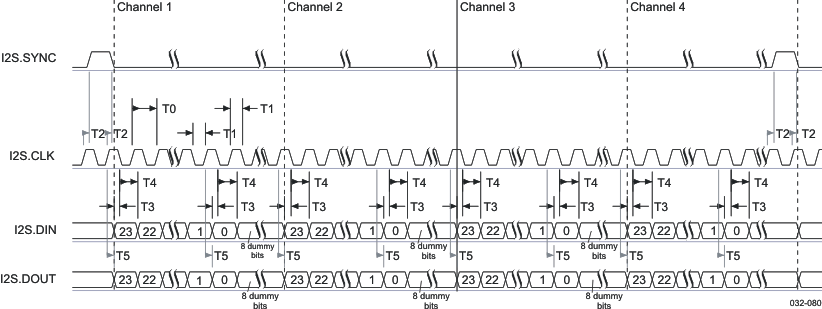 Figure 4-4 TDM Interface—TDM Master Mode
The timing requirements in Table 4-7 are valid on the following conditions of input slew and output load:
- Rise and fall time range of inputs (SYNC, DIN) is tR/tF = 1.0 ns/6.5 ns
- Capacitance load range of outputs (CLK, SYNC, DOUT) is CLoad = 1 pF/30 pF
Table 4-7 lists the master mode timing requirements for the TDM interface.
Table 4-7 TDM Interface Master Mode Timing Requirements
| Notation | Parameter | Min | Max | Unit | |
|---|---|---|---|---|---|
| T3 | tsu(DIN-CLKH) | Setup time, TDM.DIN valid to TDM.CLK high | 25 | ns | |
| T4 | th(DIN-CLKH) | Hold time, TDM.DIN valid from TDM.CLK high | 0 | ns | |
Table 4-8 lists the master mode switching characteristics of the TDM interface.
Table 4-8 TDM Interface Master Mode Switching Characteristics
| Notation | Parameter | Min | Max | Unit | |
|---|---|---|---|---|---|
| T0 | tc(CLK) | Cycle time, TDM.CLK (1) | 1/64 * Fs | ns | |
| T1 | tw(CLK) | Pulse duration, TDM.CLK high or low(2) | 0.45*P | 0.55*P | ns |
| T2 | td(CLKL-SYNC) | Delay time, TDM.CLK rising edge to TDM.SYNC transition | –10 | 10 | ns |
| T5 | td(CLKL-DOUT) | Delay time, TDM.CLK rising edge to TDM.DOUT transition | –10 | 12 | ns |
4.7.5 Voice/Bluetooth PCM Interfaces
The PCM interface transfers voice data at 8-kHz (default narrowband mode) or 16-kHz (wideband mode) sample rates. The CM interface can act as a slave or master. No PLL is used for the PCM interface, but dividers are used to derive the 8- or 16-kHz clock from HFCLKIN (only when HFCLKIN = 26 MHz). If the system master clock is not 26 MHz, the voice PCM interface is not available.
For the Bluetooth interface, the PCM is supported to transfer voice data to the Bluetooth chip at 8-kHz (default narrowband mode) or 16-kHz sample rate.
The TPS65950 acts as a master for the Bluetooth interface. The frame synchronization and the bit clock are shared from the voice PCM interface. If the system master clock is not 26 MHz, the Bluetooth interface is not available.
Two modes are available for the PCM interfaces: mode 1 (writing on the PCM_VCK rising edge) and mode 2 (writing on the PCM_VCK falling edge).
Table 4-9 and Table 4-10 assume testing over the recommended operating conditions (see Figure 4-5 and Figure 4-6).
 Figure 4-5 Voice/BT PCM Interface—Master Mode (Mode 1)
 Figure 4-6 Voice PCM Interface—Slave Mode (Mode 1)
The timing requirements in Table 4-9 are valid on the following conditions of input slew and output load:
- Rise and fall time range of inputs (SYNC, DIN) is tR/tF = 1.0 ns/6.5 ns
- Capacitance load range of outputs (CLK, SYNC, DOUT) is CLoad = 1 pF/30 pF
Table 4-9 lists the timing requirements for the voice PCM interface, mode 1.
Table 4-9 Voice PCM Interface Timing Requirements (Mode 1)
| Notation | Parameter | Min | Max | Unit | |
|---|---|---|---|---|---|
| Voice/Bluetooth PCM Master Mode | |||||
| P3 | tsu(VDR-VCK) | Setup time, PCM.VDR valid to PCM. VCK transition (1) | 30 | ns | |
| P4 | th(VDR-VCK) | Hold time, PCM.VDR valid from PCM.VCK transition(1) | 0 | ns | |
| Voice PCM Slave Mode | |||||
| P0 | tc(VCK) | Cycle time, PCM.VCK(2) | 1/(33 to 65 * Fs) | ns | |
| P1 | tw(VCK) | Pulse duration, PCM.VCK high or low(3) | 0.45 * P | 0.55 * P | ns |
| P3 | tsu(VDR-VCK) | Setup time, PCM.VDR valid to PCM. VCK transition(1) | 10 | ns | |
| P4 | th(VDR-VCK) | Hold time, PCM.VDR valid from PCM. VCK transition(1) | 5 | ns | |
| P6 | th(VFS-VCK) | Hold time, PCM.VFS valid from PCM.VCK transition(1) | 5 | ns | |
| P7 | tSU(VFS-VCK) | Setup time, PCM.VFS valid to PCM. VCK transition (1) | 10 | ns | |
Table 4-10 lists the switching characteristics of the voice PCM interface, mode 1.
Table 4-10 Voice PCM Interface Switching Characteristics (Mode 1)
| Notation | Parameter | Min | Max | Unit | |
|---|---|---|---|---|---|
| Voice/Bluetooth PCM Master Mode | |||||
| P0 | tc(VCK) | Cycle time, PCM.VCK(1) | 1/65 * Fs | ns | |
| P1 | tw(VCK) | Pulse duration, PCM.VCK high or low(2) | 0.45 * P | 0.55 * P | ns |
| P2 | td(VCK-VFS) | Delay time, PCM.VCK transition to PCM.VFS transition (3) | –10 | 10 + Pvoice | ns |
| P5 | td(VCL-VDX) | Delay time, PCM.VCK transition to PCM.VDX transition | –10 | 10 | ns |
| Voice PCM Slave Mode | |||||
| P5 | td(VCL-VDX) | Delay time, PCM.VCK transition to PCM.VDX transition | 0 | 20 | ns |
4.7.6 JTAG Interfaces
The TPS65950 Joint Test Action Group (JTAG) test access port (TAP) controller handles standard IEEE JTAG interfaces. This section describes the timing requirements for the tools used to test TPS65950 power management.
The JTAG/TAP module provides a JTAG interface according to IEEE Standard 1149.1a. This interface uses the four I/O pins TMS, TCK, TDI, and TDO. The TMS, TCK, and TDI inputs contain a pullup device, which makes their state high when they are not driven. The output TDO is a 3-state output, which is high impedance except when data are shifted between TDI and TDO:
- TCK is the test clock signal.
- TMS is the test mode select signal.
- TDI is the scan path input.
- TDO is the scan path output.
TMS and TDO are multiplexed at the top level with the GPIO0 and GPIO1 pins. The dedicated external test pin switches from functional mode (GPIO0 and GPIO1) to JTAG mode (TMS and TDO). The JTAG operations are controlled by a state-machine that follows the IEEE Standard 1149.1a state diagram. This state-machine is reset by the TPS65950 internal power-on reset (POR). A test mode is selected by writing a 6-bit word (instruction) into the instruction register and then accessing the related data register.
Table 4-11 and Table 4-12 assume testing over the recommended operating conditions (see Figure 4-7). The input timing requirements are given by considering a rising or falling edge of 7 ns. The capacitive load is 35 pF.
 Figure 4-7 JTAG Interface Timing
Table 4-11 JTAG Interface Timing Requirements
| Notation | Parameter | Min | Max | Unit | |
|---|---|---|---|---|---|
| Clock | |||||
| JL1 | tc(TCK) | Cycle time, JTAG.TCK period | 30 | ns | |
| JL2 | tw(TCK) | Pulse duration, JTAG.TCK high or low(1) | 0.48*P | 0.52*P | ns |
| Read Timing | |||||
| JL3 | tsu(TDIV-TCKH) | Setup time, JTAG.TDI valid before JTAG.TCK high | 8 | ns | |
| JL4 | th(TDIV-TCKH) | Hold time, JTAG.TDI valid after JTAG.TCK high | 5 | ns | |
| JL5 | tsu(TMSV-TCKH) | Setup time, JTAG.TMS valid before JTAG.TCK high | 8 | ns | |
| JL6 | th(TMSV-TCKH) | Hold time, JTAG.TMS valid after JTAG.TCK high | 5 | ns | |
Table 4-12 JTAG Interface Switching Characteristics
| Notation | Parameter | Min | Max | Unit | |
|---|---|---|---|---|---|
| Write Timing | |||||
| JL7 | td(TCK-TDOV)) | Delay time, JTAG, TCK active edge to JTAG.TDO valid | 0 | 14 | ns |