SLVSCK1A April 2014 – April 2014 TPS65980
PRODUCTION DATA.
- 1 Features
- 2 Applications
- 3 Description
- 4 Simplified Schematic
- 5 Revision History
- 6 Pin Configuration and Functions
- 7 Specifications
- 8 Detailed Description
- 9 Application and Implementation
- 10Power Supply Recommendations
- 11Layout
- 12Device and Documentation Support
- 13Mechanical, Packaging, and Orderable Information
Package Options
Mechanical Data (Package|Pins)
- RHF|24
Thermal pad, mechanical data (Package|Pins)
Orderable Information
11 Layout
11.1 Layout Guidelines
Proper placement and routing will maximize the performance of the TPS65980. Follow Figure 23 for optimized layout and routing (hashed planes indicate bottom layer).
11.2 Layout Example
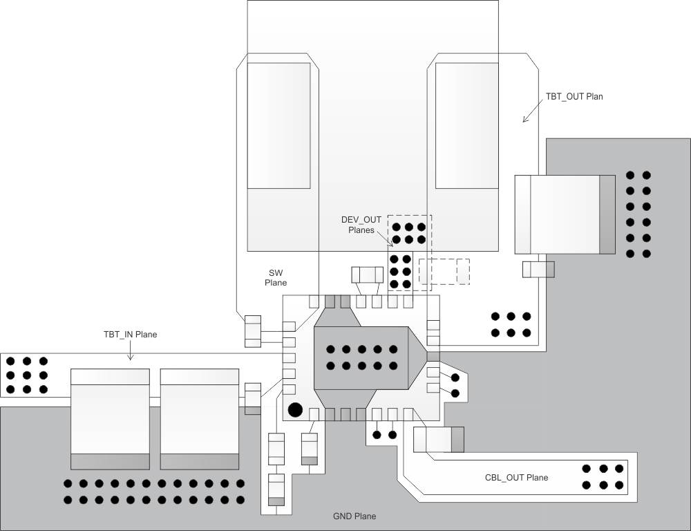 Figure 23. Top View Board Layout
For TBT_IN, the input capacitors must be placed close to the device with an inductance less than 1nH from input capacitors to the TBT_IN pins. Layout tools and calculators are available to approximate the inductance. The input capacitors must have their GND side area via stitched to the GND plane. The GND side of the input cap should also share the same polygon as the PGND/PowerPad on the top layer. PowerPad should be connected to the GND plane through multiple vias.
Inductor placement should be above the TPS65980, slightly to the left of the device. The SW pins to the inductor must be connected though a plane as shown in Figure 23. The TBT_OUT pins also have to be connected to the other side of the inductor with a plane. This plane should be wide to overlap the output capacitors. The GND side of the output capacitors should be stitched to the GND plane.
The CBL_OUT output capacitor should be placed close to the device on the top layer with an inductance less than 1 nH from the capacitor to the CBL_OUT pin. The DEV_OUT capacitor is best placed on the bottom side of the board with two planes (top and bottom) connect through a set of vias. The number of vias placed should be able to carry at least 3 A (DEV_OUT = 2.5 A max) for margin and inductance path less than 1nH from DEV_OUT pins to capacitor. When routing DEV_OUT to an internal power plane, follow Figure 24 for via paths.
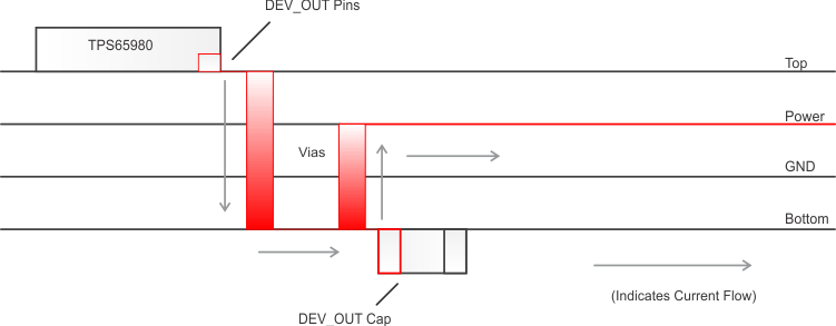 Figure 24. DEV_OUT Recommended Routing
The charge pump capacitor must be placed on the top layer close to the CPP and CPN pins. The inductance paths from capacitor to the pins must be less than 1 nH. SS and Compensation components should be placed on the top layer close to the device.