SLVSCK1A April 2014 – April 2014 TPS65980
PRODUCTION DATA.
- 1 Features
- 2 Applications
- 3 Description
- 4 Simplified Schematic
- 5 Revision History
- 6 Pin Configuration and Functions
- 7 Specifications
- 8 Detailed Description
- 9 Application and Implementation
- 10Power Supply Recommendations
- 11Layout
- 12Device and Documentation Support
- 13Mechanical, Packaging, and Orderable Information
Package Options
Mechanical Data (Package|Pins)
- RHF|24
Thermal pad, mechanical data (Package|Pins)
Orderable Information
7 Specifications
7.1 Absolute Maximum Ratings
over operating free-air temperature (unless otherwise noted)(1)| MIN | MAX | UNIT | |||
|---|---|---|---|---|---|
| Input voltage range(2) | TBT_IN | –0.3 | 18 | V | |
| DEV_EN | –0.3 | 3.6 | |||
| BOOT | –0.3 | 25 | |||
| BOOT (10 ns transient) | –0.3 | 27 | |||
| BOOT (vs SW) | –0.3 | 7 | |||
| SW | –0.6 | 18 | |||
| SW (10 ns transient) | –2 | 20 | |||
| COMP | –0.3 | 3.6 | |||
| SS | –0.3 | 3.6 | |||
| CBL_ILIMIT | –0.3 | 3.6 | |||
| CPP | –0.3 | 7.2 | |||
| CPN | –0.3 | 3.6 | |||
| Output voltage range(2) | TBT_OUT, CBL_OUT, DEV_OUT | –0.3 | 3.6 | V | |
| RESET, HV_OK | –0.3 | 3.6 | |||
| Vdiff | Voltage from GND to Thermal Pad | –0.2 | 0.2 | V | |
| Voltage from PGND to GND | –0.2 | 0.2 | V | ||
| TA | Operating ambient temperature | –40 | 85 | °C | |
| TJ | Operating junction temperature | –40 | 125 | °C | |
7.2 Handling Ratings
| MIN | MAX | UNIT | |||
|---|---|---|---|---|---|
| Tstg | Storage temperature range | –55 | 150 | °C | |
| V(ESD) | Electrostatic discharge | Human body model (HBM), per ANSI/ESDA/JEDEC JS-001, all pins(1) | 0 | 2 | kV |
| Charged device model (CDM), per JEDEC specification JESD22-C101, all pins(2) | 0 | 500 | V | ||
7.3 Recommended Operating Conditions
over operating free-air temperature (unless otherwise noted)| MIN | MAX | UNIT | |||
|---|---|---|---|---|---|
| TBT_IN | Supply input voltage range | 2.5 | 15.75 | V | |
| VI | Input voltage range | DEV_EN | –0.1 | 3.6 | |
| BOOT | –0.1 | 25 | |||
| SW | –0.6 | 16.5 | |||
| COMP | –0.1 | 3.6 | |||
| SS | –0.1 | 3.6 | |||
| CBL_ILIMIT | –0.1 | 3.6 | |||
| CPP | –0.1 | 7.2 | |||
| CPN | –0.1 | 3.6 | |||
| VO | Output voltage range | TBT_OUT, CBL_OUT, DEV_OUT | –0.1 | 3.6 | V |
| RESET, HV_OK | –0.1 | 3.6 | |||
| TA | Operating free-air temperature | –40 | 85 | °C | |
| TJ | Operating junction temperature | –40 | 125 | °C | |
7.4 Thermal Information
| THERMAL METRIC(1) | TPS65980 | UNIT | |
|---|---|---|---|
| RHF | |||
| 24 PIN | |||
| RθJA | Junction-to-ambient thermal resistance | 30.1 | °C/W |
| RθJC(top) | Junction-to-case (top) thermal resistance | 26.9 | |
| RθJB | Junction-to-board thermal resistance | 8.2 | |
| ψJT | Junction-to-top characterization parameter | 0.3 | |
| ψJB | Junction-to-board characterization parameter | 8.2 | |
| RθJC(bot) | Junction-to-case (bottom) thermal resistance | 1.5 | |
7.5 Electrical Characteristics
Unless otherwise noted all specifications applies over the VTBT_IN range and operating ambient temperature of–40°C ≤ TA ≤ 85°C, CTBT_IN = 22 µF, CTBT_OUT = 10 µF, CCBL_OUT = 1 µF, CSS = 10 nF, and 33 V/µs logic input transitions. Typical values are for VTBT_IN = 12 V and TA = 25°C.
| PARAMETER | TEST CONDITIONS | MIN | TYP | MAX | UNIT | |
|---|---|---|---|---|---|---|
| POWER SUPPLIES AND CURRENTS | ||||||
| VTBT_IN | TBT_IN Input voltage range | 2.5 | 12 | 15.75 | V | |
| VREF_RSTN | TBT_OUT to RESET clear high | TBT_OUT rising | 3 | 3.1 | 3.2 | V |
| TBT_OUT to RESET assert low | TBT_OUT falling | 2.5 | 2.6 | 2.7 | ||
| VHVTR | TBT_IN to HV_OK assert | TBT_IN rising | 4.36 | 4.5 | 4.64 | V |
| VHVTHYST | TBT_IN to HV_OK clear | TBT_IN Falling hysteresis | 100 | mV | ||
| SR02L | TBT_IN Input slew rate | TBT_IN transition from 0 V to 3.3 V | 0.1 | 30 | kV/s | |
| SRL2H | TBT_IN Input slew rate | TBT_IN transition from 3.3 V to 15 V | 0.1 | 30 | kV/s | |
| IRAMP | Combined output di/dt(1) | 5 | kA/s | |||
| Efficiency | Buck converter efficiency | ILOADTOTAL = 3 A, VTBT_IN = 12 V | 87% | |||
| Charge pump efficiency | VTBT_IN = 3.3 V, ILOADTOTAL = 25 mA | 47% | ||||
| POWER OUTPUT PINS (LOW VOLTAGE INPUT)(2) | ||||||
| VTBT_IN | TBT_IN Input voltage range | 2.5 | 3.3 | 3.4 | V | |
| VTBT_OUT | TBT_OUT Output voltage range(3) | 3.135 | 3.25 | 3.4 | V | |
| ITBT_OUT | TBT_OUT Load current(4)(5) | RESET high | 5 | 50 | mA | |
| RESET low | 100 | µA | ||||
| POWER OUTPUT PINS (HIGH VOLTAGE INPUT)(6) | ||||||
| VTBT_IN | TBT_IN Input voltage range | 10 | 12 | 15.75 | V | |
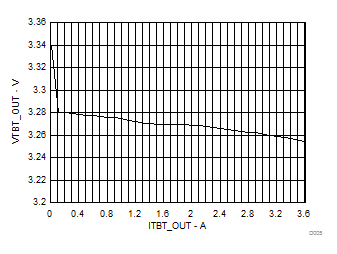
| VTBT_OUT | TBT_OUT Output voltage range(3) | I_LOADTOTAL = 1 A to 3.5 A | 3.221 | 3.27 | 3.319 | V |
| I_LOADTOTAL = 0.235 A to 3.5 A | 3.221 | 3.27 | 3.42 | |||
| ITBT_OUT | TBT_OUT Load current(4) | 235 | 1000 | mA | ||
| VCBL_OUT | CBL_OUT Output voltage range(3) | ILIMIT = 0, ICBL_OUT = 0 to 720 mA | 3.171 | 3.27 | 3.319 | V |
| ILIMIT = 1, ICBL_OUT = 0 to 1.44 A | 3.12 | 3.27 | 3.319 | |||
| VDEV_OUT | DEV_OUT Output Voltage Range | IDEV_OUT = 0 to 2500 mA | 3 | 3.27 | 3.319 | V |
| POWER OUTPUT PINS (HIGH VOLTAGE INPUT DURING SYSTEM SLEEP) | ||||||
| VTBT_IN | TBT_IN Input voltage range | 5.2 | 12 | 15.75 | V | |
| VTBT_OUT | TBT_OUT DC Output voltage range | I_LOADTOTAL = 1 A to 3.5 A | 3.221 | 3.27 | 3.319 | V |
| I_LOADTOTAL = 0.235 A to 3.5 A | 3.221 | 3.27 | 3.42 | |||
| ITBT_OUT | TBT_OUT Load current | 5 | 31 | mA | ||
| VCBL_OUT | CBL_OUT Output voltage range(3) | ICBL_OUT = 0 to 235 mA | 3.171 | 3.27 | 3.319 | V |
| VDEV_OUT | DEV_OUT Output voltage range | IDEV_OUT = 0 to 700 mA | 3 | 3.3 | 3.319 | V |
| CABLE OUTPUT (HIGH VOLTAGE INPUT & HIGH VOLTAGE INPUT DURING SLEEP) | ||||||
| VCBL_OUT_MON | CBL_OUT Ramp-up monotonicity(7) | CBL_OUT ramp from off to on | 0 | mV | ||
| VCBL_OUT_RIP | CBL_OUT Voltage ripple | After settling All output combined Load > 1 mA |
2 | %P-P | ||
| All output combined Load < 1 mA | 40 | mVP=P | ||||
| ILIM_CBLOUT | CBL_OUT Current limit | ILIMIT = 0 | 0.8 | 1.1 | 1.4 | A |
| ILIMIT = 1 | 1.6 | 2.2 | 2.8 | |||
| tLIM_CBLOUT | Short circuit response time | RCBL_OUT = 0.5 Ω to GND, ILIMIT = 0 | 500 | µs | ||
| RCBL_OUT = 0.01 Ω to GND, ILIMIT = 0 | 8 | |||||
| DEV_EN AND ILIMIT INPUT LOGIC | ||||||
| VIH | High-level input voltage | 2.6 | V | |||
| VIL | Low-level input voltage | 0.6 | V | |||
| IIN | Input leakage to GND | VDEV_EN = 3.3V | 1 | mA | ||
| RESET AND HV_OK OUTPUT LOGIC | ||||||
| VOH | High-level output voltage | IL = –1.5 mA, Referenced to VTBT_OUT | –250 | 0 | mV | |
| VOL | Low-level output voltage | IL = 1.5 mA | 0 | 250 | mV | |
| SOFT START(3) | ||||||
| IINRUSH | Inrush current di/dt | 250 | kA/s | |||
| THERMAL SHUTDOWN | ||||||
| TSD | Shutdown temperature | 120 | 135 | 150 | °C | |
| TSDHYST | Shutdown hysteresis | 10 | °C | |||
7.6 Timing Requirements
| MIN | TYP | MAX | UNIT | |||
|---|---|---|---|---|---|---|
| tIN2OR | TBT_IN to TBT_OUT On Time | VTBT_IN ≥ 0.9 × VTBT_IN(min) to VTBT_OUT ≥ 0.99 × VTBT_OUT(min) RTBT_OUT = 100 Ω |
20 | ms | ||
| tIN2OF | TBT_IN to TBT_OUT Off Time | VTBT_IN ≤ 0.9 × VTBT_IN(min) to VTBT_OUT ≤ 0.1 × VTBT_OUT(min) RTBT_OUT = 100 Ω |
2.4 | 4 | ms | |
| tOUT2RR | TBT_OUT to RESETZ High time | VTBT_OUT ≥ VREF_RSTN(max) rising to VRESET = 0.9 × VOH, CRESETN = 100 pF |
20 | µs | ||
| tIN2RF | TBT_IN to RESETZ Low time | VTBT_IN ≤ 0.9 × VTBT_IN(min) to VRESET = 0.1 × VOH, CRESETN = 100 pF |
20 | ms | ||
| tHV2OKR | TBT_IN Rise to HV_OK | VTBT_IN ≥ VHVTR to VHV_OK = 0.9 × VOH CHV_OK = 100 pF |
10 | µs | ||
| tHV2OKF | TBT_IN Fall to HV_OK | VTBT_IN ≤ VHVTR-VHVTHYST to VHV_OK = 0.1 × VOH, CHV_OK = 100 pF |
10 | µs | ||
| tHV2CR(1)(2) | HV_OK to CBL_OUT On time | VHV_OK ≥ 1.65 V to VCBL_OUT = 2.95 V RCB_OUT = 100 Ω, CHV_OK = 100 pF |
0.1 | 10 | ms | |
| tHV2CF | HV_OK to CBL_OUT Off time | VHV_OK ≤ 1.65 V to VCBL_OUT = 2.95 V RCB_OUT = 100 Ω, CHV_OK = 100 pF |
40 | µs | ||
| tRCBL | CABLE_OUT Ramp time | VCBL_OUT ramp 10% to 90% CCBL_OUT = 0 to 52 µF |
0.1 | 10 | ms | |
| tDEVEN | DEV_EN to DEV_OUT On time | VDEV_EN ≤ 1.65 V to VDEV_OUT = 2.7 V RDEV_OUT = 100 Ω |
0.1 | 10 | ms | |
| tDEVDIS | DEV_EN to DEV_OUT Off time | VDEV_EN ≥ 1.65V to VDEV_OUT = 2.7 V RDEV_OUT = 100 Ω |
50 | ms | ||
| tHV2DEVEN | Wait time from HV_OK High before DEV_EN can be asserted low(2) | VHV_OK ≥ 1.65 V to VDEV_EN ≤ 1.65 V CHV_OK = 100 pF |
2 | ms | ||
7.7 Timing Diagrams
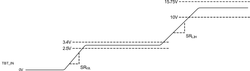 Figure 1. TBT_IN Slew Rates
The TPS65980 has two normal operating regions. The first region is when 2.5 V ≤ VTBT_IN ≤ 3.4 V. This is the normal power-up state and is termed the low-voltage state. When the input transitions to this range, the input slew rate must meet the SR02L limits. In this voltage range, the TPS65980 operates with a charge pump to generate the nominally 3.3 V output. When the input voltage moves to the higher end of this range, the buck converter takes over to produce the 3.3 V. In normal operation, the TPS65980 input voltage will transition from the low-voltage range to a high-voltage range where 10 V ≤ VTBT_IN ≤ 15.75 V. This is the high-voltage state and is the state where the TPS65980 will operate most of the time. In this state, the device operates as a buck converter providing a nominally 3.3 V output. Figure 1 shows the input voltage transitions and states.
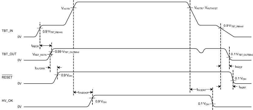 Figure 2. Timing Diagram
Figure 2 shows normal operating timing diagram for the TBT_OUT output voltage and the RESET and HV_OK output indicator signals. When TBT_IN transitions to the low-voltage range, TBT_OUT will power up a short time later. Once TBT_OUT reaches the normal output range, RESET will transition high. However, timing for RESET is measured from the input TBT_IN transitioning high. When TBT_IN transitions from the low-voltage input range to the high-voltage input range, HV_OK will transition high. RESET is an active-high output indicating that the TBT_OUT voltage is valid and. HV_OK is an active-high output indicating that the TBT_IN voltage is in the high-voltage range. When in the high-voltage state, the TPS65980 can provide much higher output current than when in the low-voltage state.
When the TBT_IN input transitions from high-voltage to low-voltage, HV_OK will de-assert to a logic low. When the TBT_IN input voltage falls below the minimum operating voltage, the RESET output will de-assert low.
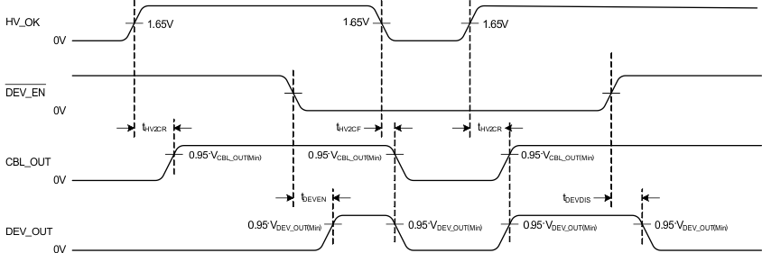 Figure 3. Timing Diagram
Figure 3 shows the CBL_OUT and DEV_OUT outputs and timing based on the HV_OK signal and the DEV_ENZ input. The CBL_OUT output will be connected to TBT_OUT and supplying 3.3V when HV_OK is asserting high. The DEV_OUT output will be connected to TBT_OUT and supplying 3.3 V when HV_OK is asserting high and the DEV_ENZ input is low.
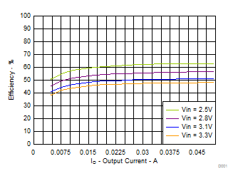
7.8 Typical Characteristics
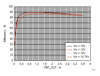
| VIN = 12V | ||
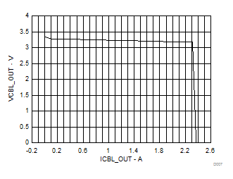
| VIN = 12V | CBL_ILIMIT = 1 |
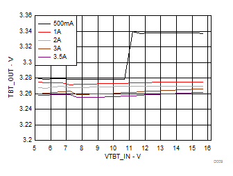
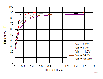
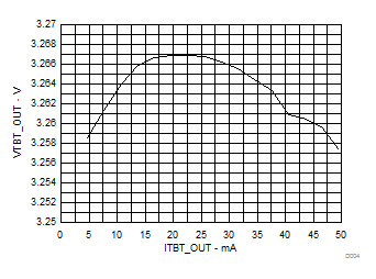
| VIN = 3.3V | ||
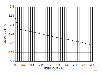
| VIN = 12V | ||
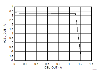
| VIN = 12V | CBL_ILIMIT = 0 |