SLVSFN8B September   2020  – October 2022 TPS65987DDK

PRODUCTION DATA  

  1. Features
  2. Applications
  3. Description
  4. Revision History
  5. Pin Configuration and Functions
  6. Specifications
    1. 6.1  Absolute Maximum Ratings
    2. 6.2  ESD Ratings
    3. 6.3  Recommended Operating Conditions
    4. 6.4  Thermal Information
    5. 6.5  Power Supply Requirements and Characteristics
    6. 6.6  Power Consumption Characteristics
    7. 6.7  Power Switch Characteristics
    8. 6.8  Cable Detection Characteristics
    9. 6.9  USB-PD Baseband Signal Requirements and Characteristics
    10. 6.10 Thermal Shutdown Characteristics
    11. 6.11 Oscillator Characteristics
    12. 6.12 I/O Characteristics
    13. 6.13 I2C Requirements and Characteristics
    14. 6.14 SPI Controller Timing Requirements
    15. 6.15 HPD Timing Requirements
    16. 6.16 Typical Characteristics
  7. Parameter Measurement Information
  8. Detailed Description
    1. 8.1 Overview
    2. 8.2 Functional Block Diagram
    3. 8.3 Feature Description
      1. 8.3.1  USB-PD Physical Layer
        1. 8.3.1.1 USB-PD Encoding and Signaling
        2. 8.3.1.2 USB-PD Bi-Phase Marked Coding
        3. 8.3.1.3 USB-PD Transmit (TX) and Receive (Rx) Masks
        4. 8.3.1.4 USB-PD BMC Transmitter
        5. 8.3.1.5 USB-PD BMC Receiver
      2. 8.3.2  Power Management
        1. 8.3.2.1 Power-On and Supervisory Functions
        2. 8.3.2.2 VBUS LDO
        3. 8.3.2.3 Supply Switch Over
      3. 8.3.3  Port Power Switches
        1. 8.3.3.1 PP_HV Power Switch
          1. 8.3.3.1.1 PP_HV Overcurrent Clamp
          2. 8.3.3.1.2 PP_HV Overcurrent Protection
          3. 8.3.3.1.3 PP_HV OVP and UVP
          4. 8.3.3.1.4 PP_HV Reverse Current Protection
        2. 8.3.3.2 Schottky for Current Surge Protection
        3. 8.3.3.3 PP_EXT Power Path Control
        4. 8.3.3.4 PP_CABLE Power Switch
          1. 8.3.3.4.1 PP_CABLE Overcurrent Protection
          2. 8.3.3.4.2 PP_CABLE Input Good Monitor
        5. 8.3.3.5 VBUS Transition to VSAFE5V
        6. 8.3.3.6 VBUS Transition to VSAFE0V
      4. 8.3.4  Cable Plug and Orientation Detection
        1. 8.3.4.1 Configured as a DFP
        2. 8.3.4.2 Configured as a UFP
        3. 8.3.4.3 Configured as a DRP
        4. 8.3.4.4 Fast Role Swap Signaling
      5. 8.3.5  Dead Battery Operation
        1. 8.3.5.1 Dead Battery Advertisement
        2. 8.3.5.2 BUSPOWER (ADCIN1)
      6. 8.3.6  ADC
      7. 8.3.7  DisplayPort HPD
      8. 8.3.8  Digital Interfaces
        1. 8.3.8.1 General GPIO
        2. 8.3.8.2 I2C
        3. 8.3.8.3 SPI
      9. 8.3.9  Digital Core
      10. 8.3.10 I2C Interfaces
        1. 8.3.10.1 I2C Interface Description
        2. 8.3.10.2 I2C Clock Stretching
        3. 8.3.10.3 I2C Address Setting
        4. 8.3.10.4 Unique Address Interface
        5. 8.3.10.5 I2C Pin Address Setting (ADCIN2)
      11. 8.3.11 SPI Controller Interface
      12. 8.3.12 Thermal Shutdown
      13. 8.3.13 Oscillators
    4. 8.4 Device Functional Modes
      1. 8.4.1 Boot
      2. 8.4.2 Power States
  9. Application and Implementation
    1. 9.1 Application Information
    2. 9.2 Typical Applications
      1. 9.2.1 USB4 Device Application with Host Charging
        1. 9.2.1.1 Design Requirements
          1. 9.2.1.1.1 Power Supply Design Requirements
        2. 9.2.1.2 Detailed Design Procedure
          1. 9.2.1.2.1 USB Power Delivery Source Capabilities
          2. 9.2.1.2.2 USB Power Delivery Sink Capabilities
          3. 9.2.1.2.3 Supported Data Modes
          4. 9.2.1.2.4 USB4 Hub Controller & PD Controller I2C Communication
          5. 9.2.1.2.5 Dock Management Controller & PD Controller I2C Communication
          6. 9.2.1.2.6 SPI Flash Options
  10. 10Power Supply Recommendations
    1. 10.1 3.3-V Power
      1. 10.1.1 VIN_3V3 Input Switch
      2. 10.1.2 VBUS 3.3-V LDO
    2. 10.2 1.8-V Power
    3. 10.3 Recommended Supply Load Capacitance
  11. 11Layout
    1. 11.1 Layout Guidelines
      1. 11.1.1 Top TPS65987DDK Placement and Bottom Component Placement and Layout
    2. 11.2 Layout Example
    3. 11.3 Component Placement
    4. 11.4 Routing PP_HV1/2, VBUS, PP_CABLE, VIN_3V3, LDO_3V3, LDO_1V8
    5. 11.5 Routing CC and GPIO
    6. 11.6 Thermal Dissipation for FET Drain Pads
  12. 12Device and Documentation Support
    1. 12.1 Device Support
      1. 12.1.1 Firmware Warranty Disclaimer
    2. 12.2 Documentation Support
      1. 12.2.1 Related Documentation
    3. 12.3 Support Resources
    4. 12.4 Trademarks
    5. 12.5 Electrostatic Discharge Caution
    6. 12.6 Glossary
  13. 13Mechanical, Packaging, and Orderable Information

Package Options

Mechanical Data (Package|Pins)
Thermal pad, mechanical data (Package|Pins)
Orderable Information

Routing CC and GPIO

Routing the CC lines with a 8-mil trace will ensure the needed current for supporting powered Type-C cables through VCONN. For more information on VCONN refer to the Type-C specification. For capacitor GND pin use a 16-mil trace if possible.

Most of the GPIO signals can be fanned out on the top layer with a 4-mil trace. The PP_EXT1/2 GPIO control go through a via to be routed on another layer.

Figure 11-10 below shows the CC and GPIO routing.
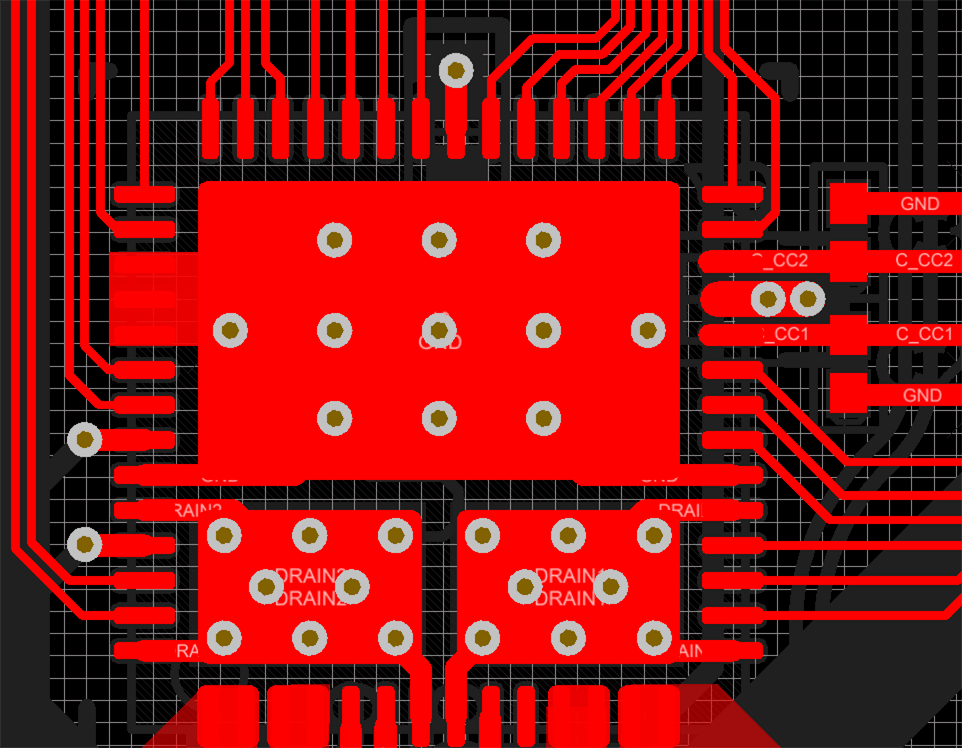
GUID-67D3B2D4-DEC4-4FDC-B630-AFFF900B6AB5-low.gifFigure 11-10 CC Routing and GPIO Fan-Out
Table 11-1 Routing Widths
ROUTEWIDTH (mil minimum)
CC1, CC2, PP_CABLE1, PP_CABLE28
VIN_3V3, LDO_3V3, LDO_1V86
Component GND10
GPIO4