SBVS340 June 2017 TPS715A-NM
PRODUCTION DATA.
- 1 Features
- 2 Applications
- 3 Description
- 4 Pin Configuration and Functions
- 5 Specifications
- 6 Detailed Description
- 7 Application and Implementation
- 8 Power Supply Recommendations
- 9 Layout
- 10Device and Documentation Support
- 11Mechanical, Packaging, and Orderable Information
Package Options
Mechanical Data (Package|Pins)
- DRB|8
Thermal pad, mechanical data (Package|Pins)
- DRB|8
Orderable Information
7 Application and Implementation
NOTE
Information in the following applications sections is not part of the TI component specification, and TI does not warrant its accuracy or completeness. TI’s customers are responsible for determining suitability of components for their purposes. Customers should validate and test their design implementation to confirm system functionality.
7.1 Application Information
The TPS715A-NM family of LDO regulators is optimized for ultralow-power applications such as the MSP430 microcontroller. The ultralow-supply current of the TPS715A-NM device maximizes efficiency at light loads, and its high input voltage range makes the device suitable for supplies such as unconditioned solar panels.
7.2 Typical Applications
7.2.1 Typical Application (Fixed-Voltage Version)
 Figure 16. Typical Application Circuit (Fixed-Voltage Version)
7.2.1.1 Design Requirements
7.2.1.1.1 Power the MSP430 Microcontroller
Several versions of the TPS715A-NM are ideal for powering the MSP430 microcontroller. Table 2 shows potential applications of some voltage versions.
Table 2. Typical MSP430 Applications
| DEVICE | VOUT (TYP) | APPLICATION |
|---|---|---|
| TPS715A19 | 1.9 V | VOUT(min) > 1.8 V required by many MSP430s. Allows lowest power consumption operation. |
| TPS715A23 | 2.3 V | VOUT(min) > 2.2 V required by some MSP430s flash operation. |
| TPS715A30 | 3 V | VOUT(min) > 2.7 V required by some MSP430s flash operation. |
| TPS715A345 | 3.45 V | VOUT(max) < 3.6 V required by some MSP430s. Allows highest speed operation. |
The TPS715A-NM family of devices offers many output voltage versions to allow the supply voltage to be optimized for the MSP430, thereby minimizing the supply current consumed by the MSP430.
7.2.1.2 Detailed Design Procedure
7.2.1.2.1 External Capacitor Requirements
Although not required, a 0.047-μF or larger input bypass capacitor, connected between IN and GND and located close to the device, is recommended to improve transient response and noise rejection of the power supply as a whole. A higher-value input capacitor may be necessary if large, fast-rise-time load transients are anticipated and the device is located several inches from the power source.
The TPS715A-NM device requires an output capacitor connected between OUT and GND to stabilize the internal control loop. Any capacitor (including ceramic and tantalum) greater than or equal to 0.47 μF properly stabilizes this loop. The X7R- or X5R-type capacitors are recommended because these capacitors have a wider temperature specification and lower temperature coefficient, but other types of capacitors can be used.
7.2.1.2.2 Dropout Voltage (VDO)
Generally speaking, the dropout voltage often refers to the voltage difference between the input and output voltage (VDO = VIN – VOUT). However, in the Electrical Characteristics table, VDO is defined as the VIN – VOUT voltage at the rated current, where the pass-FET is fully enhanced in the ohmic region of operation and is characterized by the classic RDS(on) of the FET. VDO indirectly specifies a minimum input voltage above the nominal programmed output voltage at which the output voltage is expected to remain within its accuracy boundary. If the input falls below this VDO limit (VIN < VOUT + VDO), then the output voltage decreases to follow the input voltage.
Dropout voltage is always determined by the RDS(on) of the main pass-FET. Therefore, if the LDO operates below the rated current, then the VDO for that current scales accordingly. RDS(on) can be calculated using Equation 1.

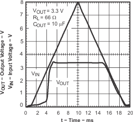
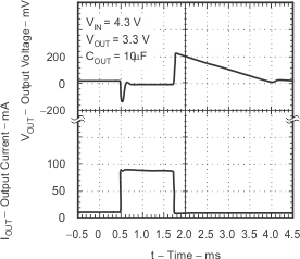
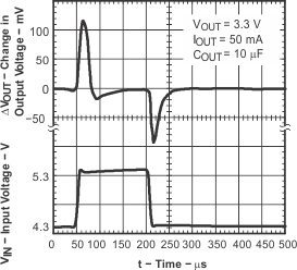
7.2.1.3 Application Curves


7.2.2 TPS715A01 Adjustable LDO Regulator Programming
 Figure 20. TPS715A01 Adjustable LDO Regulator Programming
7.2.2.1 Detailed Design Procedure
7.2.2.1.1 Setting VOUT for the TPS715A01 Adjustable LDO
The TPS715A-NM family of devices contains an adjustable-version, the TPS715A01 device, that sets the output voltage using an external resistor divider as shown in Figure 20. The output voltage operating range is 1.2 V to 15 V, and is calculated using Equation 2.

where
- VREF = 1.205 V (typical)
Choose resistors R1 and R2 to allow approximately 1.5-μA of current through the resistor divider. Lower value resistors can be used for improved noise performance, but consume more power. Avoid higher resistor values because leakage current into or out of FB across R1, R2 creates an offset voltage that is proportional to VOUT divided by VREF. The recommended design procedure is to choose R2 = 1 MΩ to set the divider current at 1.5 μA, and then calculate R1 using Equation 3.

Figure 20 shows this configuration.
7.3 Do's and Don'ts
Place at least one 0.47-µF capacitor as close as possible to the OUT and GND pins of the regulator.
Do not connect the output capacitor to the regulator using a long, thin trace.
Connect an input capacitor of 0.047 µF as close as possible to the IN and GND pins of the regulator for best performance.
Do not exceed the absolute maximum ratings.