SBVS340 June 2017 TPS715A-NM
PRODUCTION DATA.
- 1 Features
- 2 Applications
- 3 Description
- 4 Pin Configuration and Functions
- 5 Specifications
- 6 Detailed Description
- 7 Application and Implementation
- 8 Power Supply Recommendations
- 9 Layout
- 10Device and Documentation Support
- 11Mechanical, Packaging, and Orderable Information
Package Options
Mechanical Data (Package|Pins)
- DRB|8
Thermal pad, mechanical data (Package|Pins)
- DRB|8
Orderable Information
6 Detailed Description
6.1 Overview
The TPS715A-NM family of low dropout regulators consumes only 3.2 µA of current and offers a wide input voltage range and low-dropout voltage in a small package. The devices operate over an input range of 2.5 V to 24 V and are stable with any capacitor greater than or equal to 0.47 μF. The low quiescent current makes the TPS715A-NM ideal for powering battery management devices. Specifically, because the TPS715A-NM is enabled as soon as the applied voltage reaches the minimum input voltage, the output is quickly available to power continuously-operating, battery-charging devices.
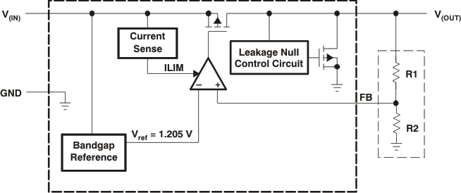
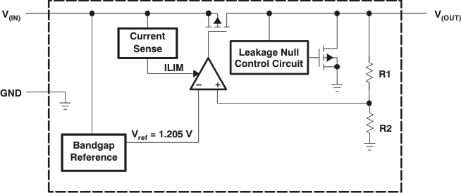
6.2 Functional Block Diagrams
 Figure 14. Functional Block Diagram—Adjustable Version
 Figure 15. Functional Block Diagram—Fixed Version
6.3 Feature Description
6.3.1 Wide Supply Range
This device has an operational input supply range of 2.5 V to 24 V, allowing for a wide range of applications. This wide supply range is ideal for applications that have either large transients or high dc voltage supplies.
6.3.2 Low Supply Current
This device only requires 3.2 µA (typical) of supply current and has a maximum current consumption of 5.8 µA at –40°C to 125°C.
6.3.3 Stable With Any Capacitor ≥ 0.47 µF
Any capacitor, including both ceramic and tantalum, greater than or equal to 0.47 μF properly stabilizes this loop.
6.3.4 Internal Current Limit
The internal current limit circuit is used to protect the LDO against high-load current faults or shorting events. The LDO is not designed to operate in a steady-state current limit. During a current limit event, the LDO sources constant current. Therefore, the output voltage falls when load impedance decreases.
NOTE
If a current limit occurs and the resulting output voltage is low, excessive power is dissipated across the LDO, resulting in possible damage to the device.
6.3.5 Reverse Current
The TPS715A-NM device PMOS-pass transistor has a built-in back diode that conducts current when the input voltage drops below the output voltage (for example, during power down). Current is conducted from the output to the input and is not internally limited. If extended reverse voltage operation is anticipated, external limiting may be required.
6.4 Device Functional Modes
Table 1 provides a quick comparison between the normal, dropout, and disabled modes of operation.
Table 1. Device Functional Mode Comparison
| OPERATING MODE | PARAMETER | |
|---|---|---|
| VIN | IOUT | |
| Normal | VIN > VOUT(nom) + VDO | IOUT < ICL |
| Dropout | VIN < VOUT(nom) + VDO | IOUT < ICL |
| Disabled | — | — |
6.4.1 Normal Operation
The device regulates to the nominal output voltage under the following conditions:
- The input voltage is greater than the nominal output voltage plus the dropout voltage (VOUT(nom) + VDO).
- The output current is less than the current limit (IOUT < ICL).
- The device junction temperature is less than 125°C.
6.4.2 Dropout Operation
If the input voltage is lower than the nominal output voltage plus the specified dropout voltage, but all other conditions are met for normal operation, the device operates in dropout mode. In this mode, the output voltage tracks the input voltage. During this mode, the transient performance of the device becomes significantly degraded because the pass device is in the linear region and no longer controls the current through the LDO. Line or load transients in dropout can result in large output-voltage deviations.