SLVSAI3A September 2010 – May 2016
PRODUCTION DATA.
- 1 Features
- 2 Applications
- 3 Description
- 4 Revision History
- 5 Pin Configuration and Functions
- 6 Specifications
- 7 Detailed Description
- 8 Application and Implementation
- 9 Power Supply Recommendations
- 10Layout
- 11Device And Documentation Support
- 12Mechanical, Packaging, And Orderable Information
Package Options
Mechanical Data (Package|Pins)
Thermal pad, mechanical data (Package|Pins)
Orderable Information
7 Detailed Description
7.1 Overview
The TPS736xx-Q1 belongs to a family of new-generation LDO regulators that use an NMOS pass transistor to achieve ultra-low dropout performance, reverse current blockage, and freedom from output capacitor constraints. These features, combined with low noise and an enable input, make the TPS736xx-Q1 ideal for portable applications. This regulator family offers a wide selection of fixed output voltage versions and an adjustable output version. All versions have thermal and overcurrent protection, including foldback current limit.
7.2 Functional Block Diagrams
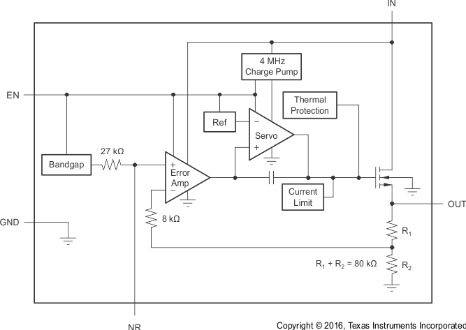
 Figure 29. Fixed Voltage Version
Table 1. Standard 1% Resistor Values for Common Output Voltages
| VOUT(1) | R1 | R2 |
|---|---|---|
| 1.2 V | Short | Open |
| 1.5 V | 23.2 kΩ | 95.3 kΩ |
| 1.8 V | 28 kΩ | 56.2 kΩ |
| 2.5 V | 39.2 kΩ | 36.5 kΩ |
| 2.8 V | 44.2 kΩ | 33.2 kΩ |
| 3 V | 46.4 kΩ | 30.9 kΩ |
| 3.3 V | 52.3 kΩ | 30.1 kΩ |
7.3 Feature Description
7.3.1 Internal Current Limit
The TPS736xx-Q1 internal current limit helps protect the regulator during fault conditions. Foldback current limit helps to protect the regulator from damage during output short-circuit conditions by reducing current limit when VOUT drops below 0.5 V (see Figure 10). Approximately –0.2 V of VOUT results in a current limit of 0 mA. Therefore, if OUT is forced below –0.2 V before EN goes high, the device may not start up. In applications that work with both a positive and negative voltage supply, the TPS736xx-Q1 must be enabled first.
7.3.2 Transient Response
The low open-loop output impedance provided by the NMOS pass element in a voltage follower configuration allows operation without an output capacitor for many applications. As with any regulator, the addition of a capacitor (nominal value of 1 μF) from the OUT pin to ground reduces undershoot magnitude but increase its duration. In the adjustable version, the addition of a capacitor, CFB, from the OUT pin to the FB pin also improves the transient response.
The TPS736xx-Q1 does not have active pulldown when the output is overvoltage. This allows applications that connect higher voltage sources, such as alternate power supplies, to the output. This also results in an output overshoot of several percent if load current quickly drops to zero when a capacitor is connected to the output. The duration of overshoot can be reduced by adding a load resistor. The overshoot decays at a rate determined by output capacitor COUT and the internal and external load resistance. The rate of decay is given by Equation 1 or Equation 2, determined by the version.


7.3.3 Reverse Current
The NMOS pass element of the TPS736xx-Q1 provides inherent protection against current flow from the output of the regulator to the input when the gate of the pass device is pulled low. To ensure that all charge is removed from the gate of the pass element, the EN pin must be driven low before the input voltage is removed. If this is not done, the pass element may be left on due to stored charge on the gate.
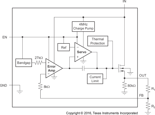
After the EN pin is driven low, no bias voltage is needed on any pin for reverse current blocking. The reverse current is specified as the current flowing out of the IN pin due to voltage applied on the OUT pin. There is additional current flowing into the OUT pin due to the 80-kΩ internal resistor divider to ground (see Figure 29 and Figure 30).
For the TPS73601, reverse current may flow when VFB is more than 1 V above VIN.
7.3.4 Thermal Protection
Thermal protection disables the output when the junction temperature rises to approximately 160°C, allowing the device to cool. When the junction temperature cools to approximately 140°C, the output circuitry is again enabled. Depending on power dissipation, thermal resistance, and ambient temperature, the thermal protection circuit may cycle on and off. This limits the dissipation of the regulator, protecting it from damage due to overheating.
Any tendency to activate the thermal protection circuit indicates excessive power dissipation or an inadequate heat sink. For reliable operation, junction temperature must be limited to 125°C maximum. To estimate the margin of safety in a complete design (including heat sink), increase the ambient temperature until the thermal protection is triggered; use worst-case loads and signal conditions. For good reliability, thermal protection must trigger at least 35°C above the maximum expected ambient condition of your application. This produces a worst-case junction temperature of 125°C at the highest expected ambient temperature and worst-case load.
The internal protection circuitry of the TPS736xx-Q1 has been designed to protect against overload conditions. It was not intended to replace proper heat sinking. Continuously running the TPS736xx-Q1 into thermal shutdown degrades device reliability.
7.4 Device Functional Modes
7.4.1 Enable Pin and Shutdown
The enable pin (EN) is active high and is compatible with standard TTL-CMOS levels. A VEN below 0.5 V (maximum) turns the regulator off and drops the GND pin current to approximately 10 nA. When EN is used to shutdown the regulator, all charge is removed from the pass transistor gate, and the output ramps back up to a regulated VOUT (see Figure 21).
When shutdown capability is not required, EN can be connected to VIN. However, the pass gate may not be discharged using this configuration, and the pass transistor may be left on (enhanced) for a significant time after VIN has been removed. This scenario can result in reverse current flow (if the IN pin is low impedance) and faster ramp times upon power-up. In addition, for VIN ramp times slower than a few milliseconds, the output may overshoot upon power-up.
Current limit foldback can prevent device start-up under some conditions. See the Internal Current Limit section for more information.
7.4.2 Dropout Voltage
The TPS736xx-Q1 uses an NMOS pass transistor to achieve extremely low dropout. When (VIN – VOUT) is less than the dropout voltage (VDO), the NMOS pass device is in its linear region of operation and the input-to-output resistance is the RDS(ON) of the NMOS pass element.
For large step changes in load current, the TPS736xx-Q1 requires a larger voltage drop from VIN to VOUT to avoid degraded transient response. The boundary of this transient dropout region is approximately twice the DC dropout. Values of VIN – VOUT above this line ensure normal transient response.
Operating in the transient dropout region can cause an increase in recovery time. The time required to recover from a load transient is a function of the magnitude of the change in load current rate, the rate of change in load current, and the available headroom (VIN to VOUT voltage drop). Under worst-case conditions [full-scale instantaneous load change with (VIN – VOUT) close to DC dropout levels], the TPS736xx-Q1 can take a couple of hundred microseconds to return to the specified regulation accuracy.
