SBVS083E January 2007 – January 2015 TPS780
PRODUCTION DATA.
- 1 Features
- 2 Applications
- 3 Description
- 4 Revision History
- 5 Pin Configuration and Functions
- 6 Specifications
- 7 Detailed Description
- 8 Application and Implementation
- 9 Power Supply Recommendations
- 10Layout
- 11Device and Documentation Support
- 12Mechanical, Packaging, and Orderable Information
Package Options
Mechanical Data (Package|Pins)
Thermal pad, mechanical data (Package|Pins)
- DRV|6
Orderable Information
7 Detailed Description
7.1 Overview
The TPS780 family of low-dropout regulators (LDOs) is designed specifically for battery-powered applications where ultralow quiescent current is a critical parameter. The absence of pulldown circuitry at the output of the LDO provides the flexibility to use the regulator output capacitor as a temporary backup power supply for a short period of time (for example, during battery replacement). The TPS780 family is compatible with the TI MSP430 and other similar products. The enable pin (EN) is compatible with standard CMOS logic. This LDO family is stable with any output capacitor greater than 1.0 µF.
7.2 Functional Block Diagram
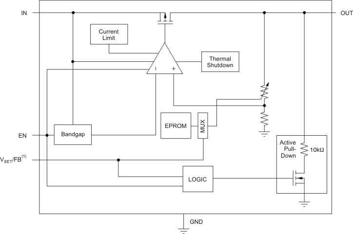
7.3 Feature Description
7.3.1 Internal Current Limit
The TPS780 is internally current-limited to protect the regulator during fault conditions. During current limit, the output sources a fixed amount of current that is largely independent of output voltage. For reliable operation, do not operate the device in a current-limit state for extended periods of time.
The PMOS pass element in the TPS780 family has a built-in body diode that conducts current when the voltage at OUT exceeds the voltage at IN. This current is not limited, so if extended reverse voltage operation is anticipated, external limiting to 5% of rated output current may be appropriate.
7.3.2 Shutdown
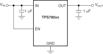
The enable pin (EN) is active high and is compatible with standard and low-voltage CMOS levels. When shutdown capability is not required, connect EN to the IN pin, as shown in Figure 54.
7.3.3 Active VOUT Pulldown
In the TPS780 series, the active pulldown discharges VOUT when the device is off. However, the input voltage must be greater than 2.2 V for the active pulldown to work.
7.4 Device Functional Modes
Table 1 provides a quick comparison between the normal, dropout, and disabled modes of operation.
Table 1. Device Functional Mode Comparison
| OPERATING MODE | PARAMETER | |||
|---|---|---|---|---|
| VIN | EN | IOUT | TJ | |
| Normal | VIN > VOUT(nom) + VDO | VEN > VEN(HI) | IOUT < ICL | TJ < TSD |
| Dropout | VIN < VOUT(nom) + VDO | VEN > VEN(HI) | IOUT < ICL | TJ < TSD |
| Disabled | — | VEN < VEN(LO) | — | TJ > TSD |
7.4.1 Normal Operation
The device regulates to the nominal output voltage under the following conditions:
- The input voltage is greater than the nominal output voltage plus the dropout voltage (VOUT(nom) + VDO).
- The enable voltage has previously exceeded the enable rising threshold voltage (VEN > VEN(HI)) and not yet decreased below the enable falling threshold.
- The output current is less than the current limit (IOUT < ICL).
- The device junction temperature is less than the thermal shutdown temperature (TJ < TSD).
7.4.2 Dropout Operation
If the input voltage is lower than the nominal output voltage plus the specified dropout voltage, but all other conditions are met for normal operation, the device operates in dropout mode. In this mode, the output voltage tracks the input voltage. During this mode, the transient performance of the device becomes significantly degraded because the pass device is in a triode state and no longer controls the current through the LDO. Line or load transients in dropout can result in large output-voltage deviations.
7.4.3 Disabled
The device is disabled under the following conditions:
- The enable voltage is less than the enable falling threshold voltage (VEN < VEN(LO)) or has not yet exceeded the enable rising threshold.
- The device junction temperature is greater than the thermal shutdown temperature (TJ > TSD).
7.5 Programming
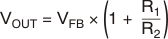
7.5.1 Programming the TPS78001 Adjustable LDO Regulator
The output voltage of the TPS78001 adjustable regulator is programmed using an external resistor divider as shown in Figure 55. The output voltage operating range is 1.2 V to 5.1 V, and is calculated using Equation 1:
where
- VFB = 1.216 V typical (the internal reference voltage)
Resistors R1 and R2 should be chosen for approximately 1.2-μA divider current. Lower value resistors can be used for improved noise performance, but the solution consumes more power. Higher resistor values should be avoided because leakage current into/out of FB across R1/R2 creates an offset voltage that artificially increases/decreases the feedback voltage and thus erroneously decreases/increases VOUT. Table 2 lists several common output voltages and resistor values. The recommended design procedure is to choose R2 = 1 MΩ to set the divider current at 1.2 μA, and then calculate R1 using Equation 2:
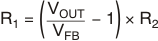
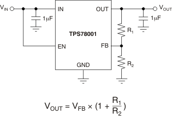 Figure 55. TPS78001 Adjustable LDO Regulator Programming
Table 2. Output Voltage Programming Guide
| OUTPUT VOLTAGE | R1 | R2 |
|---|---|---|
| 1.8 V | 0.499 MΩ | 1 MΩ |
| 2.8 V | 1.33 MΩ | 1 MΩ |
| 5.0 V | 3.16 MΩ | 1 MΩ |