SBVS083E January 2007 – January 2015 TPS780
PRODUCTION DATA.
- 1 Features
- 2 Applications
- 3 Description
- 4 Revision History
- 5 Pin Configuration and Functions
- 6 Specifications
- 7 Detailed Description
- 8 Application and Implementation
- 9 Power Supply Recommendations
- 10Layout
- 11Device and Documentation Support
- 12Mechanical, Packaging, and Orderable Information
Package Options
Mechanical Data (Package|Pins)
Thermal pad, mechanical data (Package|Pins)
- DRV|6
Orderable Information
5 Pin Configuration and Functions
SON
6 Pins
Top View
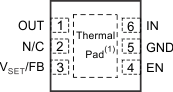
1. It is recommended that the SON package thermal pad be connected to ground.
SOT
5 Pins
Top View
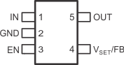
Pin Functions
| PIN | I/O | DESCRIPTION | ||
|---|---|---|---|---|
| NAME | SON | SOT | ||
| OUT | 1 | 5 | O | Regulated output voltage pin. A small (1-μF) ceramic capacitor is needed from this pin to ground to assure stability. See Input and Output Capacitor Requirements for more details. |
| N/C | 2 | — | — | Not connected. |
| VSET/FB | 3 | 4 | I | Feedback pin (FB) for adjustable versions; VSET for fixed voltage versions. Drive the select pin (VSET) below 0.4 V to select preset output voltage high. Drive the VSET pin over 1.2 V to select preset output voltage low. |
| EN | 4 | 3 | I | Enable pin. Drive this pin over 1.2 V to turn on the regulator. Drive this pin below 0.4 V to put the regulator into shutdown mode, reducing operating current to 18 nA typical. |
| GND | 5 | 2 | — | Ground pin. Tie all ground pins to ground for proper operation. |
| IN | 6 | 1 | I | Input pin. A small capacitor is needed from this pin to ground to assure stability. A typical input capacitor is 1.0 μF. Tie back both input and output capacitor ground to the IC ground, with no significant impedance between them. |
| Thermal pad | — | — | — | (SON package only) Connect the thermal pad to ground. |