SBVS083E January 2007 – January 2015 TPS780
PRODUCTION DATA.
- 1 Features
- 2 Applications
- 3 Description
- 4 Revision History
- 5 Pin Configuration and Functions
- 6 Specifications
- 7 Detailed Description
- 8 Application and Implementation
- 9 Power Supply Recommendations
- 10Layout
- 11Device and Documentation Support
- 12Mechanical, Packaging, and Orderable Information
Package Options
Mechanical Data (Package|Pins)
Thermal pad, mechanical data (Package|Pins)
- DRV|6
Orderable Information
9 Power Supply Recommendations
For best performance, connect a low-output impedance power supply directly to the IN pin of the TPS780. Inductive impedances between the input supply and the IN pin create significant voltage excursions at the IN pin during start-up or load transient events. If inductive impedances are unavoidable, use an input capacitor.
9.1 Powering the MSP430 Microcontroller
Several versions of the TPS780 are ideal for powering the MSP430 microcontroller. Table 4 shows potential applications of some voltage versions.
Table 4. Typical MSP430 Applications
| DEVICE | VOUT(HI)
(TYP) |
VOUT(LO)
(TYP) |
APPLICATION |
|---|---|---|---|
| TPS780360200 | 3.6 V | 2.0 V | VOUT, MIN > 1.800 V required by many MSP430s. Allows lowest power consumption operation. |
| TPS780360220 | 3.6 V | 2.2 V | VOUT, MIN > 2.200 V required by some MSP430s FLASH operation. |
| TPS780360300 | 3.6 V | 3.0 V | VOUT, MIN > 2.700 V required by some MSP430s FLASH operation. |
| TPS780360220 | 3.6 V | 2.2 V | VOUT, MIN < 3.600 V required by some MSP430s. Allows highest speed operation. |
The TPS780 family offers many output voltage versions to allow designers to optimize the supply voltage for the processing speed required of the MSP430. This flexible architecture minimizes the supply current consumed by the particular MSP430 application. The MSP430 total system power can be reduced by substituting the 500-nA IQ TPS780 series LDO in place of an existing ultralow IQ LDO (typical best case = 1 μA). Additionally, DVS allows for increasing the clock speed in active mode (MSP430 VCC = 3.6 V). The 3.6-V VCC reduces the MSP430 time in active mode. In low-power mode, MSP430 system power can be further reduced by lowering the MSP430 VCC to 2.2 V in sleep mode.
Key features of the TPS780 series are an ultralow quiescent current (500 nA), DVS, and miniaturized packaging. The TPS780 family are available in SON-6 and TSOT-23 packages. Figure 59 shows a typical MSP430 circuit powered by an LDO without DVS. Figure 60 is an MSP430 circuit using a TPS780 LDO that incorporates an integrated DVS, thus simplifying the circuit design. In a circuit without DVS, as Figure 59 illustrates, VCC is always at 3.0 V. When the MSP430 goes into sleep mode, VCC remains at 3.0 V; if DVS is applied, VCC could be reduced in sleep mode. In Figure 60, the TPS780 LDO with integrated DVS maintains 3.6-V VCC until a logic high signal from the MSP430 forces VOUT to level shift VOUT from 3.6 V down to 2.2 V, thus reducing power in sleep mode.
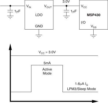 Figure 59. Typical LDO Without DVS
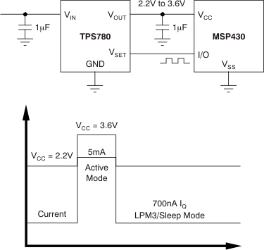 Figure 60. TPS780 With Integrated DVS
The other benefit of DVS is that it allows a higher VCC voltage on the MSP430, increasing the clock speed and reducing the active mode dwell time.
The total system power savings is outlined in Table 5, Table 6, and Table 7. In Table 5, the MSP430 power savings are calculated for various MSP430 devices using a TPS780 series with integrated DVS versus a standard ultralow IQ LDO without DVS. In Table 6, the TPS780 series quiescent power is calculated for a VIN of 4.2 V, with the same VIN used for the ultralow IQ LDO. Quiescent power dissipation in an LDO is the VIN voltage times the ground current, because zero load is applied. After the dissipation power is calculated for the individual LDOs in Table 6, simple subtraction outputs the LDO power savings using the TPS780 series. Table 7 calculates the total system power savings using a TPS780 series LDO in place of an ultralow IQ 1.2-μA LDO in an MSP430F1121 application. There are many different versions of the MSP430. Actual power savings vary depending on the selected device.
Table 5. DDV MSP430 Power Savings With the TPS780 Series on Selected MSP430 Devices
| DEVICE | LPM3 AT VCC = 3 V, IQ
(μA) |
LPM3 AT VCC = 3.0 V × IQ (μW) |
LPM3 AT VCC = 2.2 V, IQ (μA) |
LPM3 AT VCC = 2.2 V × IQ (μW) |
μW SAVINGS USING ONLY DVS |
|---|---|---|---|---|---|
| MSP430F1121 | 1.6 | 4.8 | 0.7 | 1.5 | 3.3 |
| MSP430F149 | 1.6 | 4.8 | 0.9 | 2.0 | 2.8 |
| MSP430F2131 | 0.9 | 2.7 | 0.7 | 1.5 | 1.2 |
| MSP430F249 | 1.0 | 3.0 | 0.9 | 2.0 | 1.0 |
| MSP430F413 | 0.9 | 2.7 | 0.7 | 1.5 | 1.2 |
| MSP430F449 | 1.6 | 4.8 | 1.1 | 2.4 | 2.4 |
Table 6. Typical Ultralow IQ LDO Quiescent Power Dissipation vs the TPS780 Series
| TYPICAL ULTRALOW IQ LDO AT 25°C AMBIENT | TYPICAL ULTRALOW IQ LDO AT 25°C AMBIENT POWER DISSIPATION | TPS780 SERIES TYPICAL IQ AT 25°C AMBIENT | TPS780 SERIES AT 25°C AMBIENT, POWER DISSIPATION | MSP430 SYSTEM POWER SAVINGS USING THE TPS780 SERIES |
|---|---|---|---|---|
| IQ
(μA) |
IQ × VIN = 4.2 V (μW) |
TPS780 IQ
(μA) |
IQ × VIN = 4.2 V (μW) |
Quiescent Power Dissipation Savings (μW) |
| 1.20 | 5.04 | 0.42 | 1.76 | 3.28 |