SBVS097G march 2008 – june 2023 TPS799-Q1
PRODUCTION DATA
- 1
- 1 Features
- 2 Applications
- 3 Description
- 4 Revision History
- 5 Pin Configuration and Functions
- 6 Specifications
- 7 Detailed Description
- 8 Application and Implementation
- 9 Device and Documentation Support
- 10Mechanical, Packaging, and Orderable Information
Package Options
Mechanical Data (Package|Pins)
Thermal pad, mechanical data (Package|Pins)
- DRV|6
Orderable Information
8.2.2.3 Output Noise
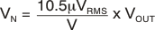
In most LDOs, the band gap is the dominant noise source. If a noise-reduction capacitor (CNR) is used with the TPS799-Q1, the band gap does not contribute significantly to noise. Instead, noise is dominated by the output resistor divider and the error amplifier input. To minimize noise in a given application, use a 0.01-μF noise reduction capacitor; for the adjustable version, smaller value resistors in the output resistor divider reduce noise. A parallel combination that gives 2 μA of divider current has the same noise performance as a fixed-voltage version. To further optimize noise, equivalent series resistance of the output capacitor can be set to approximately 0.2 Ω. This configuration maximizes phase margin in the control loop, reducing total output noise by up to 10%.
Noise can be referred to the feedback point (FB pin) such that with CNR = 0.01 μF, total noise is approximately given by Equation 1:
The adjustable version of the TPS79901-Q1 device does not have the noise-reduction pin available, so ultra-low noise operation is not possible. Noise can be minimized according to the previous recommendations.