SBVS097G march   2008  – june 2023 TPS799-Q1

PRODUCTION DATA  

  1.   1
  2. Features
  3. Applications
  4. Description
  5. Revision History
  6. Pin Configuration and Functions
  7. Specifications
    1. 6.1 Absolute Maximum Ratings
    2. 6.2 ESD Ratings
    3. 6.3 Recommended Operating Conditions
    4. 6.4 Thermal Information
    5. 6.5 Electrical Characteristics
    6. 6.6 Typical Characteristics
  8. Detailed Description
    1. 7.1 Overview
    2. 7.2 Functional Block Diagrams
    3. 7.3 Feature Description
      1. 7.3.1 Internal Current Limit
      2. 7.3.2 Shutdown
      3. 7.3.3 Dropout Voltage
      4. 7.3.4 Start-Up
      5. 7.3.5 Undervoltage Lockout (UVLO)
    4. 7.4 Device Functional Modes
  9. Application and Implementation
    1. 8.1 Application Information
    2. 8.2 Typical Application
      1. 8.2.1 Design Requirements
      2. 8.2.2 Detailed Design Procedure
        1. 8.2.2.1 Input and Output Capacitor Requirements
        2. 8.2.2.2 Feedback Capacitor Requirements (TPS79901-Q1 Only)
        3. 8.2.2.3 Output Noise
        4. 8.2.2.4 Transient Response
        5. 8.2.2.5 Minimum Load
      3. 8.2.3 Application Curve
    3. 8.3 Power Supply Recommendations
    4. 8.4 Layout
      1. 8.4.1 Layout Guidelines
        1. 8.4.1.1 Board Layout Recommendations to Improve PSRR and Noise Performance
        2. 8.4.1.2 Thermal Consideration
        3. 8.4.1.3 Power Dissipation
        4. 8.4.1.4 Package Mounting
      2. 8.4.2 Layout Example
  10. Device and Documentation Support
    1. 9.1 Documentation Support
      1. 9.1.1 Related Documentation
    2. 9.2 Receiving Notification of Documentation Updates
    3. 9.3 Support Resources
    4. 9.4 Trademarks
    5. 9.5 Electrostatic Discharge Caution
    6. 9.6 Glossary
  11. 10Mechanical, Packaging, and Orderable Information

Package Options

Mechanical Data (Package|Pins)
Thermal pad, mechanical data (Package|Pins)
Orderable Information

Description

The TPS799-Q1 low-dropout (LDO) low-power linear regulator offers excellent AC performance with very low ground current. High power-supply rejection ratio (PSRR), low noise, fast start-up, and excellent line and load transient response are provided while consuming a very low 40-μA (typical) ground current. The TPS799-Q1 is stable with ceramic capacitors and uses an advanced BiCMOS fabrication process to yield a dropout voltage of 100 mV (typical) at a 200-mA output. The TPS799-Q1 uses a precision voltage reference and feedback loop to achieve overall accuracy of 2% over all load, line, process, and temperature variations. The device is fully specified from TJ = –40°C to +125°C and is offered in low-profile, thin SOT-23 and 2-mm × 2-mm WSON packages, designed for wireless handsets and WLAN cards.

Package Information
PART NUMBER PACKAGE(1) PACKAGE SIZE(2)
TPS799-Q1 DRV (WSON, 6) 2 mm × 2 mm
DDC (SOT-23, 5) 2.9 mm × 2.8 mm
For all available packages, see the orderable addendum at the end of the data sheet.
The package size (length × width) is a nominal value and includes pins, where applicable.


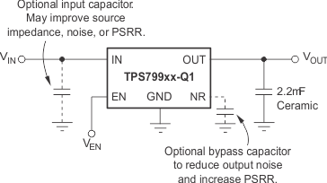
GUID-7A854105-BE2A-4223-AD70-95D5F29592EE-low.gifTypical Application Circuit Fixed Voltage Versions
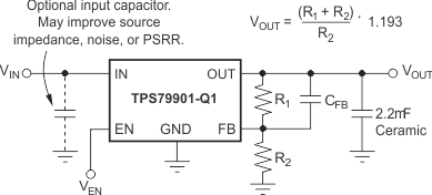
GUID-C30ADB10-BC25-40D7-84CA-7D3E1F2C1405-low.gifTypical Application Circuit Adjustable Voltage Version