SBVS171F December 2011 – October 2015 TPS7A16
PRODUCTION DATA.
- 1 Features
- 2 Applications
- 3 Description
- 4 Revision History
- 5 Pin Configuration and Functions
- 6 Specifications
- 7 Detailed Description
- 8 Application and Implementation
- 9 Power Supply Recommendations
- 10Layout
- 11Device and Documentation Support
- 12Mechanical, Packaging, and Orderable Information
Package Options
Mechanical Data (Package|Pins)
Thermal pad, mechanical data (Package|Pins)
Orderable Information
7 Detailed Description
7.1 Overview
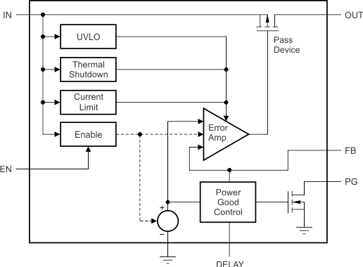
The TPS7A16 family of devices are ultralow power, low-dropout (LDO) voltage regulators that offer the benefits of ultralow quiescent current, high input voltage, and miniaturized, high thermal-performance packaging. The TPS7A16 family also offers an enable pin (EN) and integrated open-drain active-high power-good output (PG) with a user-programmable delay.
7.2 Functional Block Diagram

7.3 Feature Description
7.3.1 Enable (EN)
The enable terminal is a high-voltage-tolerant terminal. A high input on EN actives the device and turns on the regulator. For self-bias applications, connect this input to the VIN terminal.
7.3.2 Regulated Output (VOUT)
The VOUT terminal is the regulated output based on the required voltage. The output has current limitation. During initial power up, the regulator has a soft start incorporated to control the initial current through the pass element. In the event that the regulator drops out of regulation, the output tracks the input minus a drop based on the load current. When the input voltage drops below the UVLO threshold, the regulator shuts down until the input voltage recovers above the minimum start-up level.
7.3.3 Power-Good
The power-good (PG) pin is an open-drain output and can be connected to any 5-V or lower rail through an external pull-up resistor. When no CDELAY is used, the PG output is high-impedance when VOUT is greater than the PG trip threshold (VIT). If VOUT drops below VIT, the open-drain output turns on and pulls the PG output low. If output voltage monitoring is not needed, the PG pin can be left floating or connected to GND.
The power-good feature functionality is only guaranteed when VIN ≥ 3 V (VIN_(MIN))
7.3.4 PG Delay Timer (DELAY)
The power-good delay time (tDELAY) is defined as the time period from when VOUT exceeds the PG trip threshold voltage (VIT) to when the PG output is high. This power-good delay time is set by an external capacitor (CDELAY) connected from the DELAY pin to GND; this capacitor is charged from 0 V to approximately 1.8 V by the DELAY pin current (IDELAY) once VOUT exceeds the PG trip threshold (VIT).
When CDELAY is used, the PG output is high-impedance when VOUT exceeds VIT, and VDELAY exceeds VREF.
The power-good delay time can be calculated using: tDELAY = (CDELAY × VREF) / IDELAY. For example, when CDELAY = 10 nF, the PG delay time is approximately 12 ms; that is, (10 nF × 1.193 V) / 1 µA = 11.93 ms.
7.3.5 Internal Current Limit
The fixed internal current limit of the TPS7A16 family helps protect the regulator during fault conditions. The maximum amount of current the device can source is the current limit (225 mA, typical), and is largely independent of output voltage. For reliable operation, do not operate the device in current limit for extended periods of time.
7.3.6 Thermal Protection
Thermal protection disables the output when the junction temperature rises to approximately 170°C, allowing the device to cool. When the junction temperature cools to approximately 150°C, the output circuitry is enabled. Depending on power dissipation, thermal resistance, and ambient temperature, the thermal protection circuit may cycle ON and OFF. This cycling limits the dissipation of the regulator, protecting it from damage as a result of overheating.
7.4 Device Functional Modes
7.4.1 Normal Operation
The device regulates to the nominal output voltage under the following conditions:
- The input voltage is at least as high as VIN(MIN).
- The input voltage is greater than the nominal output voltage added to the dropout voltage.
- The enable voltage has previously exceeded the enable rising threshold voltage and has not decreased below the enable falling threshold.
- The output current is less than the current limit.
- The device junction temperature is less than the maximum specified junction temperature.
7.4.2 Dropout Operation
If the input voltage is lower than the nominal output voltage plus the specified dropout voltage, but all other conditions are met for normal operation, the device operates in dropout mode. In this mode of operation, the output voltage is the same as the input voltage minus the dropout voltage. The transient performance of the device is significantly degraded because the pass device (such as a bipolar junction transistor, or BJT) is in saturation and no longer controls the current through the LDO. Line or load transients in dropout can result in large output voltage deviations.
7.4.3 Disabled
The device is disabled under the following conditions:
- The enable voltage is less than the enable falling threshold voltage or has not yet exceeded the enable rising threshold.
- The device junction temperature is greater than the thermal shutdown temperature.
Table 1 lists the conditions that lead to the different modes of operation.
Table 1. Device Functional Mode Comparison
| OPERATING MODE | PARAMETER | |||
|---|---|---|---|---|
| VIN | VEN | IOUT | TJ | |
| Normal mode | VIN > VOUT(NOM) + VDO and VIN > VIN(MIN) | VEN > VEN_HI | IOUT < ILIM | TJ < 125°C |
| Dropout mode | VIN < VOUT(NOM) + VDO | VEN > VEN_HI | — | TJ < 125°C |
| Disabled mode (any true condition disables the device | — | VEN < VEN_HI | — | TJ > 170°C |