SBVS256A May 2016 – September 2016 TPS7A19
PRODUCTION DATA.
- 1 Features
- 2 Applications
- 3 Description
- 4 Revision History
- 5 Pin Configuration and Functions
- 6 Specifications
- 7 Detailed Description
- 8 Application and Implementation
- 9 Power Supply Recommendations
- 10Layout
- 11Device and Documentation Support
- 12Mechanical, Packaging, and Orderable Information
Package Options
Mechanical Data (Package|Pins)
- DRB|8
Thermal pad, mechanical data (Package|Pins)
- DRB|8
Orderable Information
7 Detailed Description
7.1 Overview
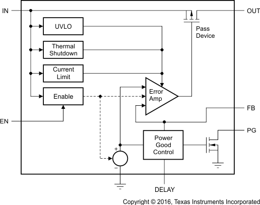
The TPS7A19 is a low-dropout linear regulator (LDO) combined with enable and power good functions. The power good pin initializes when the output voltage, VOUT, exceeds VT(PG). The power good delay is a function of the value set by an external capacitor on the DELAY pin before releasing the PG pin high.
7.2 Functional Block Diagram

7.3 Feature Description
7.3.1 Enable Pin (EN)
The enable pin is a high-voltage-tolerant pin. A logic-high input on EN actives the device and turns on the LDO. For self-bias applications, connect this input to the IN pin.
7.3.2 Regulated Output Pin (OUT)
The OUT pin is the regulated output based on the required voltage. The output is protected by internal current limiting. During initial power up, the LDO has a soft start feature incorporated to control the initial current through the pass element.
In the event that the LDO drops out of regulation, the output tracks the input minus a voltage drop based on the load current. When the input voltage drops below the UVLO threshold, the LDO shuts down until the input voltage exceeds the minimum start-up level.
7.3.3 Power-Good Pin (PG)
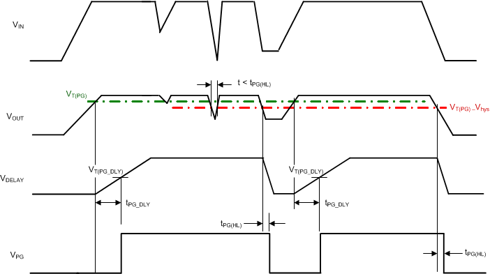
The power good pin is an output with an external pullup resistor to the regulated supply. The output remains low until the regulated VOUT exceeds approximately 91.6% of the set value, and the power good delay has expired. The regulated output falling below the 89.6% level asserts this output low after a short deglitch time of approximately 180 µs (typical).
7.3.4 Delay Timer Pin (DELAY)
An external capacitor on the DELAY pin sets the timer delay before the PG pin is asserted high. The constant output current charges an external capacitor until the voltage exceeds a threshold that trips an internal comparator. If this pin is open, the default delay time is 325 µs (typical).
The pulse delay time, tPG_DLY, is defined with the charge time of an external capacitor DELAY, as shown in Equation 1.

The PG pin initializes when VOUT exceeds 91.6% of the programmed value. The delay is a function of the value set by an external capacitor on the DELAY pin before the PG pin is released high.
 Figure 12. Conditions to Activate PG
7.3.5 Adjustable Output Voltage (ADJ for TPS7A1901)
An output voltage between 1.5 V and 18 V can be selected by using the external resistor dividers. Use Equation 2 to calculate the output voltage, where VFB = 1.233 V. In order to avoid a large leakage current and to prevent a divider error, the value of (R1 + R2) must between 10 kΩ and 100 kΩ.

7.3.6 Undervoltage Shutdown
The TPS7A19 family of devices has an internally-fixed, undervoltage-shutdown threshold. Undervoltage shutdown activates when the input voltage on VIN drops below VIN_UVLO. This activation makes sure that the regulator is not latched in an unknown state when there is a low-input supply voltage. If the input voltage has a negative transient that drops below the UVLO threshold and recovers, the regulator shuts down and powers up, similar to a typical power-up sequence when the input voltage exceeds the required levels.
7.3.7 Thermal Shutdown
The TPS7A19 incorporates a thermal shutdown (TSD) circuit as protection from overheating. For continuous standard operation, the junction temperature must not exceed the TSD trip point. If the junction temperature exceeds the TSD trip point, the output turns off. When the junction temperature falls below the TSD trip point minus the TSD hysteresis value, the output turns on again.
Thermal protection disables the output when the junction temperature rises to approximately 175°C, and allows the device to cool. When the junction temperature cools to approximately 150°C, the output circuitry enables. Based on power dissipation, thermal resistance, and ambient temperature, the thermal protection circuit may cycle on and off. This cycling limits the temperature of the regulator, and protects the device from damage as a result of overheating.
Although the internal protection circuitry of the TPS7A19 device is designed to protect against overload conditions, the circuitry is not intended to replace proper heat-sink methods. Continuously running the TPS7A19 device into thermal shutdown degrades device reliability.
7.4 Device Functional Modes
7.4.1 Operation With VIN < 4 V
The devices operate with input voltages above 4 V. The devices do not operate at input voltages below the actual UVLO voltage.
7.4.2 Operation With EN Control
The enable rising edge threshold voltage is 1.7 V, maximum. When the EN pin is held above 1.7 V, and the input voltage is greater than the UVLO rising voltage, the device enables.
The enable falling edge is 0.4 V, minimum. When the EN pin is held below 0.4 V, the device is disabled. The quiescent current is reduced in this state.