SBVS256A May 2016 – September 2016 TPS7A19
PRODUCTION DATA.
- 1 Features
- 2 Applications
- 3 Description
- 4 Revision History
- 5 Pin Configuration and Functions
- 6 Specifications
- 7 Detailed Description
- 8 Application and Implementation
- 9 Power Supply Recommendations
- 10Layout
- 11Device and Documentation Support
- 12Mechanical, Packaging, and Orderable Information
Package Options
Mechanical Data (Package|Pins)
- DRB|8
Thermal pad, mechanical data (Package|Pins)
- DRB|8
Orderable Information
6 Specifications
6.1 Absolute Maximum Ratings
over operating free-air temperature range –40°C to 125°C(unless otherwise noted)(1)| MIN | MAX | UNIT | |||
|---|---|---|---|---|---|
| Voltage(3) | Input | IN, EN | –0.3 | 45 | V |
| Output | OUT(2) | –0.3 | VIN + 0.3 | ||
| DELAY(4) | –0.3 | 45 | |||
| FB, PG | –0.3 | 22 | |||
| Current | Peak output | Internally limited | |||
| Temperature | Operating junction, TJ | –40 | 150 | °C | |
| Storage, Tstg | –65 | 150 | |||
(1) Stresses beyond those listed under absolute maximum ratings may cause permanent damage to the device. These are stress ratings only and functional operation of the device at these or any other conditions beyond those indicated under recommended operating conditions is not implied. Exposure to absolute-maximum-rated conditions for extended periods may affect device reliability.
(2) The absolute maximum rating is VIN + 0.3 V or 22 V, whichever is lower.
(3) All voltage values are with respect to GND.
(4) The voltage at the DELAY pin must be lower than the VIN voltage.
6.2 ESD Ratings
| VALUE | UNIT | |||
|---|---|---|---|---|
| V(ESD) | Electrostatic discharge | Human-body model (HBM), per ANSI/ESDA/JEDEC JS-001(1) | ±2000 | V |
| Charged-device model (CDM), per JEDEC specification JESD22-C101(2) | ±500 | |||
(1) JEDEC document JEP155 states that 500-V HBM allows safe manufacturing with a standard ESD control process.
(2) JEDEC document JEP157 states that 250-V CDM allows safe manufacturing with a standard ESD control process.
6.3 Recommended Operating Conditions
over operating free-air temperature range (unless otherwise noted)| MIN | MAX | UNIT | |||
|---|---|---|---|---|---|
| VIN | Input supply voltage | 4 | 40 | V | |
| VOUT | Output voltage | 1.5 | 18 | V | |
| VEN | Enable voltage | 0 | 40 | V | |
| TJ | Operating junction temperature | –40 | 125 | °C | |
6.4 Thermal Information
| THERMAL METRIC(1) | TPS7A19 | UNIT | |
|---|---|---|---|
| DRB (VSON) | |||
| 8 PINS | |||
| RθJA | Junction-to-ambient thermal resistance | 48 | °C/W |
| RθJC(top) | Junction-to-case (top) thermal resistance | 56.3 | °C/W |
| RθJB | Junction-to-board thermal resistance | 22.4 | °C/W |
| ψJT | Junction-to-top characterization parameter | 0.9 | °C/W |
| ψJB | Junction-to-board characterization parameter | 22.5 | °C/W |
| RθJC(bot) | Junction-to-case (bottom) thermal resistance | 4.6 | °C/W |
(1) For information about traditional and new thermal metrics, see the Semiconductor and IC Package Thermal Metrics application report.
6.5 Electrical Characteristics
at TJ = –40°C to +125°C, VIN = 14 V , VEN = VIN, IOUT = 200 μA, CIN = 22 μF, and COUT = 47 μF (unless otherwise noted)| PARAMETER | TEST CONDITIONS | MIN | TYP | MAX | UNIT | ||
|---|---|---|---|---|---|---|---|
| SUPPLY VOLTAGE AND CURRENT | |||||||
| VIN | Input voltage | VOUT ≤ 3.5 V , IOUT = 0 mA to 450 mA | 4 | 40 | V | ||
| VOUT ≥ 3.5 V , IOUT = 0 mA to 450 mA | VOUT + 0.5 | 40 | V | ||||
| IQ | Quiescent current | VIN = 4 V to 40 V, VOUT = 1.5 V, VEN = 5 V, IOUT = 0.2 mA | 15 | 25 | µA | ||
| VIN = 18.5 V to 40 V, VOUT = 18 V, VEN = 5 V, IOUT = 0.2 mA | 25 | 40 | |||||
| ISHDN | Shutdown current | VEN = 0 V, IOUT = 0 mA , VIN = 18 V, VOUT = 1.5 V | 4 | µA | |||
| VFB | Feedback voltage | Reference voltage for FB pin | 1.208 | 1.233 | 1.258 | V | |
| VIN_UVLO | Undervoltage lockout | Ramp VIN down until output is turned off | 2.6 | V | |||
| UVLOHys | Undervoltage detection hysteresis | VIN rising | 1 | V | |||
| ENABLE INPUT (EN) | |||||||
| VEN_LO | Logic input low level | 0 | 0.4 | V | |||
| VEN_HI | Logic input high level | 1.7 | V | ||||
| IEN | EN pin current | VEN = 40 V , VIN = 14 V | 1 | µA | |||
| REGULATED OUTPUT | |||||||
| VOUT | Regulated output(1) | VIN = VOUT + 1 V to 40 V and VIN ≥ 4 V, IOUT = 100 µA to 450 mA |
–2% | 2% | |||
| ΔVO(ΔVI) | Line regulation | VIN = VOUT + 1 V to 40 V and VIN ≥ 4 V, IOUT = 100 mA | 10 | mV | |||
| ΔVO(ΔIL) | Load regulation | IOUT = 1 mA to 450 mA, VIN = VOUT + 1 V and VIN ≥ 4 V | 10 | mV | |||
| VDO | Dropout voltage | VIN – VOUT, IOUT = 400 mA | 240 | 450 | mV | ||
| VIN – VOUT, IOUT = 200 mA | 160 | 300 | |||||
| IOUT | Output current | VOUT in regulation | 0 | 450 | mA | ||
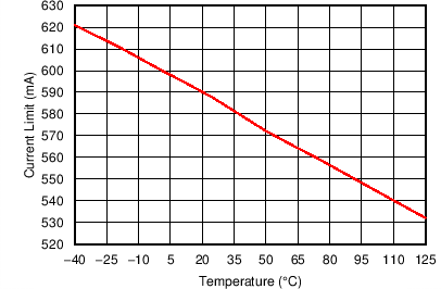
| ICL | Output current-limit | VOUT short to ground | 140 | 360 | mA | ||
| VOUT = VOUT nominal × 0.9 | 470 | 850 | |||||
| PSRR | Power-supply ripple rejection(2) | IOUT = 100 mA, COUT = 22 µF | f = 100 Hz | 60 | dB | ||
| f = 100 kHz | 40 | ||||||
| PG | |||||||
| VOL | PG output low voltage | IOL = 0.5 mA | 0.4 | V | |||
| IOH | PG leakage current | PG pulled to VOUTwith 10-kΩ resistor | 1 | µA | |||
| VT(PG) | Power good threshold | VOUT power-up | 89.6 | 91.6 | 93.6 | % of VOUT | |
| Vhys | Hysteresis | VOUT power-down | 2 | % of VOUT | |||
| PG DELAY | |||||||
| IDelay | Delay capacitor charging current | 5 | 9.5 | 14 | µA | ||
| VT(PG_DLY) | Delay pin comparator threshold voltage | 1 | V | ||||
| TEMPERATURE | |||||||
| Tsd | Junction shutdown temperature | Temperature increasing | 175 | °C | |||
| Thys | Hysteresis of thermal shutdown | 24 | °C | ||||
(1) Accuracy specification does not apply on any application condition that exceeds the power dissipation limit of the package under test. External resistor divider variation is not considered for accuracy measurement.
(2) Design information; not tested, specified by characterization.
6.6 Timing Requirements
| MIN | TYP | MAX | UNIT | |||
|---|---|---|---|---|---|---|
| TIMING FOR PG | ||||||
| tPG_DLY | Power good delay | C = delay-capacitor value capacitance = 100 nF(1) | 10.5 | ms | ||
| tPG-fixed | Power good delay | No capacitor on pin | 325 | µs | ||
| tPG(HL) | PG falling propagation delay | VOUT low to PG low | 180 | µs | ||
(1) Information only; not tested in production. The equation is based on: (C × 1) / (9.5 × 10⁻⁶) = tPG_DLY, where C = delay capacitor value capacitance; range = 100 pF to 500 nF.
6.7 Typical Characteristics
at TJ = –40°C to +125°C, VIN = 14 V , VEN = VIN, IOUT = 200 μA, CIN = 22 μF, and COUT = 47 μF (unless otherwise noted)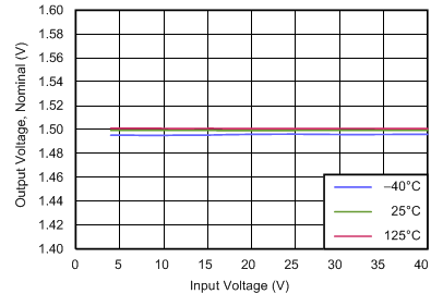
| VOUT = 1.5 V, IOUT = 100 mA | ||
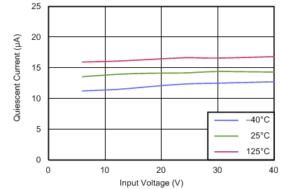
| VOUT = 1.5 V | ||
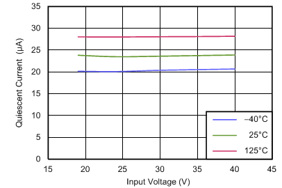
| VOUT = 18 V | ||
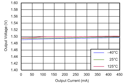
| VIN = 14 V, VOUT = 1.5 V | ||
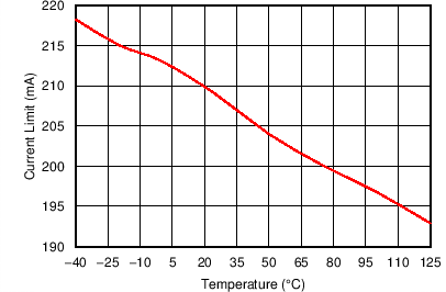
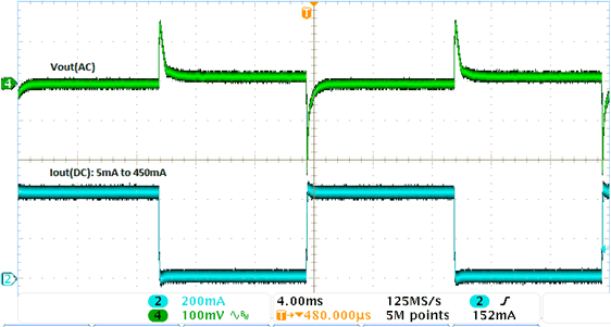
10-µF Ceramic Output Capacitor
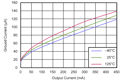
| VIN = 14 V, VOUT = 1.5 V | ||
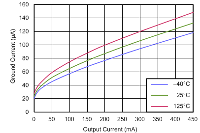
| VIN = 24 V, VOUT = 18 V | ||
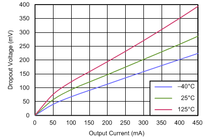
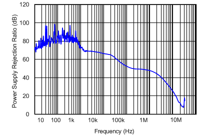
| VOUT = 5 V, COUT = 47 µF, IOUT = 10 mA | ||
