SBVS256A May 2016 – September 2016 TPS7A19
PRODUCTION DATA.
- 1 Features
- 2 Applications
- 3 Description
- 4 Revision History
- 5 Pin Configuration and Functions
- 6 Specifications
- 7 Detailed Description
- 8 Application and Implementation
- 9 Power Supply Recommendations
- 10Layout
- 11Device and Documentation Support
- 12Mechanical, Packaging, and Orderable Information
Package Options
Mechanical Data (Package|Pins)
- DRB|8
Thermal pad, mechanical data (Package|Pins)
- DRB|8
Orderable Information
8 Application and Implementation
NOTE
Information in the following applications sections is not part of the TI component specification, and TI does not warrant its accuracy or completeness. TI’s customers are responsible for determining suitability of components for their purposes. Customers should validate and test their design implementation to confirm system functionality.
8.1 Application Information
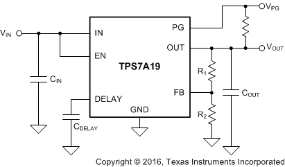
Figure 13 shows a typical application circuit for the TPS7A1901. Based on the end-application, different values of external components can be used. Some applications may require a larger output capacitor during fast load steps in order to prevent a PG low from occurring. Use a low-ESR ceramic capacitor with a dielectric of type X5R or X7R for better load transient response.
8.2 Typical Application
 Figure 13. Adjustable Operation
8.2.1 Design Requirements
For this design example, use the parameters listed in Table 1.
Table 1. Design Parameters
| DESIGN PARAMETER | EXAMPLE VALUE |
|---|---|
| Input voltage | 12 V, ±10% |
| Output voltage | 3.3 V |
| Output current | 50 mA (max) |
| PG delay time | 1 ms |
8.2.2 Detailed Design Procedure
To begin the design process:
- First, make sure that the combination of maximum current, maximum ambient temperature, maximum input voltage, and minimum output voltage does not exceed the maximum operating condition of TJ = 125°C. The Power Dissipation and Thermal Considerations section describes how to calculate the maximum ambient temperature and power dissipation.
- Next, set the feedback resistors to give the desired output voltage. See Equation 2 for the VOUT relationship to R1 and R2. A good nominal value for R2 is 10 kΩ.
- Then, calculate the required CDELAY capacitor to achieve the desired PG delay time using Equation 1. For 1 ms of delay, the nearest standard value capacitor is 10 nF.
- Finally, select an output capacitor with a total effective capacitance between 22 µF and 500 µF, a sufficient voltage rating, and an ESR below 20 Ω. Higher capacitance gives improved transient response, but results in higher inrush current at startup.
8.2.2.1 Power Dissipation and Thermal Considerations
Device power dissipation is calculated with Equation 3.

where
- PD = continuous power dissipation
- IOUT = output current
- VIN = input voltage
- VOUT = output voltage
As IQ « IOUT, the term IQ × VIN in Equation 3 can be ignored.
For a device under operation at a given ambient air temperature (TA), calculate the junction temperature (TJ) with Equation 4.

where
- θJA = junction-to-ambient air thermal impedance
A rise in junction temperature because of power dissipation can be calculated with Equation 5.

For a given maximum junction temperature (TJM), the maximum ambient air temperature (TAM) at which the device can operate is calculated with Equation 6.

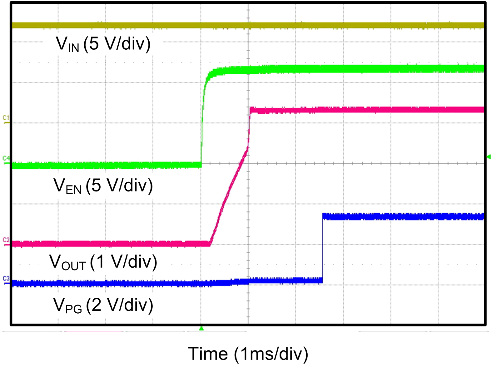
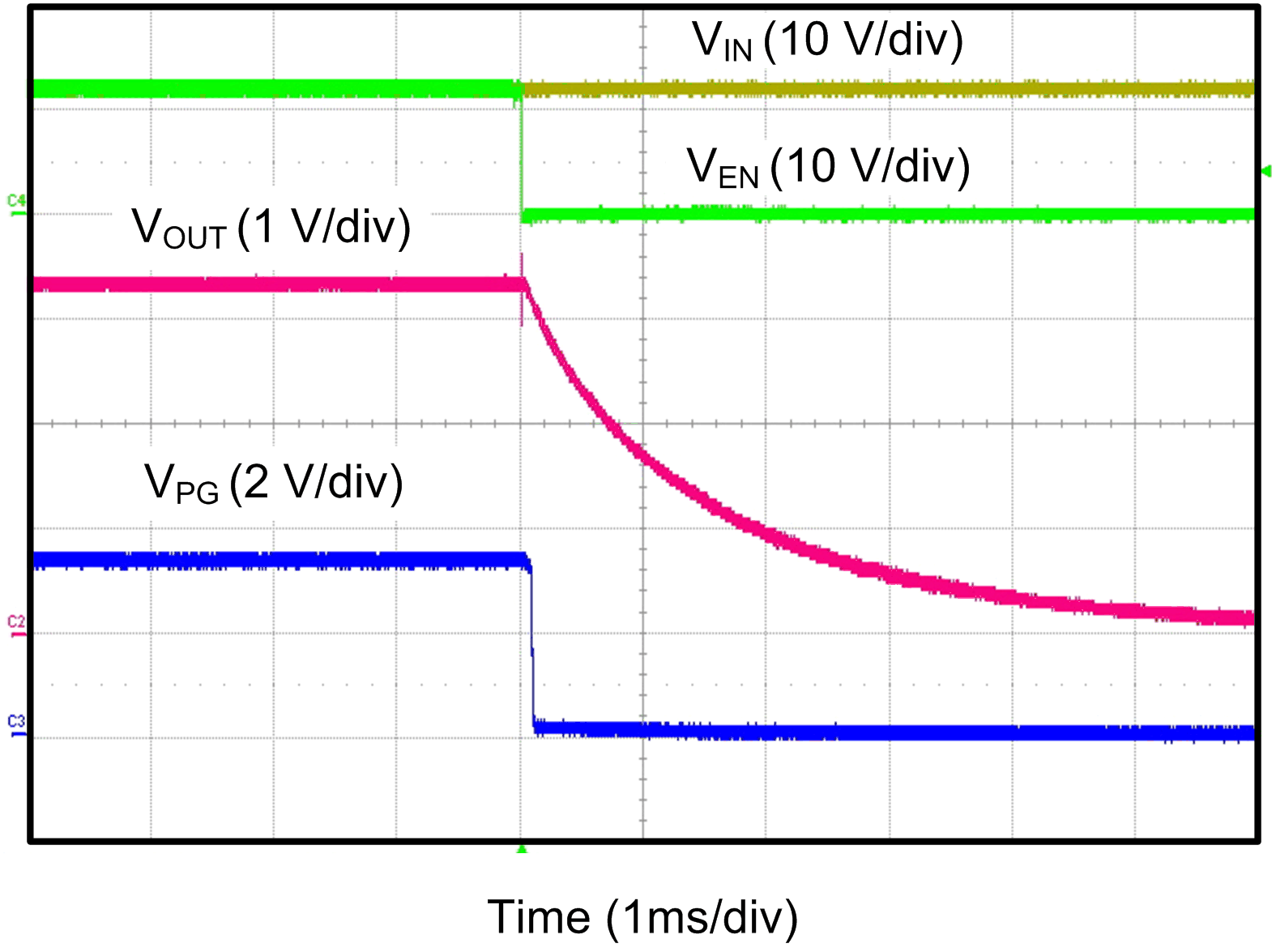
8.2.3 Application Curves

| VIN = 12 V, VEN step from 0 V to 12 V, CIN = 10 µF, COUT = 22 µF, RLOAD = 66 Ω |

| VIN = 12 V, VEN step from 12 V to 0 V, CIN = 10 µF, COUT = 22 µF, RLOAD = 66 Ω |