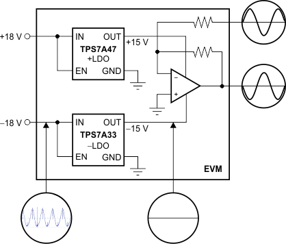
SBVS169D December 2011 – April 2015 TPS7A33
PRODUCTION DATA.
- 1 Features
- 2 Applications
- 3 Description
- 4 Revision History
- 5 Pin Configuration and Functions
- 6 Specifications
- 7 Detailed Description
-
8 Application and Implementation
- 8.1
Application Information
- 8.1.1 Adjustable Operation
- 8.1.2 Capacitor Recommendations
- 8.1.3 Input and Output Capacitor Requirements
- 8.1.4 Noise Reduction and Feed-Forward Capacitor Requirements
- 8.1.5 Post DC-DC Converter Filtering
- 8.1.6 Audio Applications
- 8.1.7 Maximum AC Performance
- 8.1.8 Power-Supply Rejection
- 8.1.9 Output Noise
- 8.1.10 Transient Response
- 8.1.11 Power for Precision Analog
- 8.2 Typical Application
- 8.3 Do's and Don’ts
- 8.1
Application Information
- 9 Power Supply Recommendations
- 10Layout
- 11Device and Documentation Support
- 12Mechanical, Packaging, and Orderable Information
Package Options
Mechanical Data (Package|Pins)
- RGW|20
Thermal pad, mechanical data (Package|Pins)
- RGW|20
Orderable Information
8 Application and Implementation
NOTE
Information in the following applications sections is not part of the TI component specification, and TI does not warrant its accuracy or completeness. TI’s customers are responsible for determining suitability of components for their purposes. Customers should validate and test their design implementation to confirm system functionality.
8.1 Application Information
8.1.1 Adjustable Operation
The TPS7A3301 has an output voltage range of –VREF to –33 V. The nominal output voltage of the device is set by two external resistors, as shown in Figure 32.
R1 and R2 can be calculated for any output voltage range using Equation 2. To ensure stability under no-load conditions at VOUT > VREF, this resistive network must provide a current equal to or greater than 5 μA.

If greater voltage accuracy is required, consider the output voltage offset contributions because of the feedback pin current and use 0.1%-tolerance resistors.
Table 2 shows the resistor combinations to achieve a few of the most common rails using commercially available, 0.1%-tolerance resistors to maximize nominal voltage accuracy while adhering to the formula shown in Equation 2.
Table 2. Suggested Resistors For Common Voltage Rails
| VOUT (V) | R1 | R2 (kΩ) | VOUT/(R1+R2) (µA) | NOMINAL ACCURACY |
|---|---|---|---|---|
| –1.171 | 0 Ω | ∞ | 0 | ±1.5% |
| –1.8 | 76.8 kΩ | 143 | 8.18 | ±(1.5% + 0.08%) |
| –3.3 | 200 kΩ | 110 | 10.64 | ±(1.5% + 0.13%) |
| –5 | 332 kΩ | 102 | 11.48 | ±(1.5% + 0.5%) |
| –10 | 1.62 MΩ | 215 | 5.44 | ±(1.5% + 0.23%) |
| –12 | 1.5 MΩ | 162 | 7.22 | ±(1.5% + 0.29%) |
| –15 | 1.24 MΩ | 105 | 11.15 | ±(1.5% + 0.18%) |
| –18 | 3.09 MΩ | 215 | 5.44 | ±(1.5% + 0.19%) |
| –24 | 1.15 MΩ | 59 | 19.84 | ±(1.5% + 0.21%) |
8.1.2 Capacitor Recommendations
Low equivalent series resistance (ESR) capacitors should be used for the input, output, noise reduction, and bypass capacitors. Ceramic capacitors with X7R and X5R dielectrics are preferred. These dielectrics offer more stable characteristics. Ceramic X7R capacitors offer improved overtemperature performance, while ceramic X5R capacitors are the most cost-effective and are available in higher values.
NOTE
8.1.3 Input and Output Capacitor Requirements
The TPS7A33 family of negative, high-voltage linear regulators achieve stability with a minimum input and output capacitance of 10 μF; however, TI highly recommends using a 47-μF capacitor to maximize AC performance.
8.1.4 Noise Reduction and Feed-Forward Capacitor Requirements
Although the noise-reduction (CNR/SS) and feed-forward (CFF) capacitors are not needed to achieve stability, TI highly recommends using a 10-nF feed-forward capacitor and a 1-μF noise-reduction capacitor to minimize noise and maximize AC performance.
The feed-forward capacitor can also provide a soft-start effect, as detailed in the application note, Pros and Cons of Using a Feed-Forward Capacitor with a Low Dropout Regulator, SBVA042 (available for download from the TI website). Figure 30 shows device start-up with no CNR/SS, CFF = 10 nF, VIN = –16 V, and VOUT = –15 V.
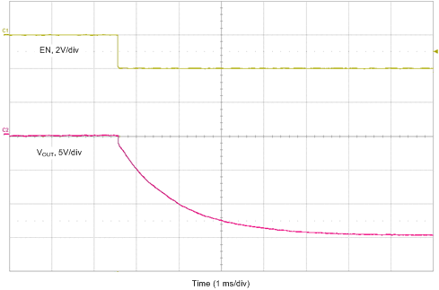 Figure 30. Start-up With a Feed-Forward Capacitor
8.1.5 Post DC-DC Converter Filtering
Most of the time, the voltage rails available in a system do not match the voltage specifications demanded by one or more of its circuits; these rails must be stepped up or down, depending on specific voltage requirements.
DC-DC converters are the preferred solution to stepping up or down a voltage rail when current consumption is not negligible. These devices offer high efficiency with minimum heat generation, but they have one primary disadvantage: they introduce a high-frequency component, and the associated harmonics, on top of the DC output signal.
If not filtered properly, this high-frequency component degrades analog circuitry performance, and reduces overall system accuracy and precision.
The TPS7A33 offers a wide-bandwidth, very-high power-supply rejection ratio (PSRR). This specification makes it ideal for post DC-DC converter filtering, as shown in Figure 31. TI highly recommends using the maximum performance schematic shown in Figure 32. Also, verify that the fundamental frequency (and its first harmonic, if possible) is within the bandwidth of the regulator PSRR, shown in Figure 16.
8.1.6 Audio Applications
Audio applications are extremely sensitive to any distortion and noise in the audio band from 20 Hz to 20 kHz. This stringent requirement demands clean voltage rails to power critical high-performance audio systems.
The very high power-supply rejection ratio (> 60 dB) and low noise at the audio band of the TPS7A33 maximize performance for audio applications; see Figure 16.
8.1.7 Maximum AC Performance
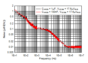
To maximize noise and PSRR performance, TI recommends including 47-μF or higher input and output capacitors, 100-nF noise-reduction capacitors, and 10-nF feed-forward capacitors, as shown in Figure 32. The solution shown delivers minimum noise levels of 16 μVRMS and power-supply rejection levels above 55 dB from 10 Hz to 1 MHz; see Figure 19.
8.1.8 Power-Supply Rejection
The 10-nF noise-reduction capacitor greatly improves TPS7A33 power-supply rejection, achieving up to 10 dB of additional power-supply rejection for frequencies between 140 Hz and 500 kHz.
Additionally, AC performance can be maximized by adding a 10-nF feed-forward capacitor (CFF) from the FB pin to the OUT pin. This capacitor greatly improves power-supply rejection at lower frequencies, for the band from 100 Hz to 100 kHz; see Figure 15.
The high power-supply rejection of the TPS7A33 makes it a good choice for powering high-performance analog circuitry.
8.1.9 Output Noise
The TPS7A33 provides low output noise when a noise-reduction capacitor (CNR/SS) is used.
The noise-reduction capacitor serves as a filter for the internal reference. By using a 10-nF noise reduction capacitor, the output noise is reduced by almost 80% (from 80 μVRMS to 17 μVRMS); see Figure 21.
The TPS7A33 low output voltage noise makes it an ideal solution for powering noise-sensitive circuitry.
8.1.10 Transient Response
As with any regulator, increasing the size of the output capacitor reduces overshoot and undershoot magnitude, but increases duration of the transient response.
8.1.11 Power for Precision Analog
One of the primary TPS7A33 applications is to provide ultralow-noise voltage rails to high-performance analog circuitry in order to maximize system accuracy and precision.
The TPS7A33 family of negative, high-voltage linear regulators provides ultralow noise, positive and negative voltage rails to high-performance analog circuitry such as operational amplifiers, ADCs, DACs, and audio amplifiers.
Because of the ultralow noise levels at high voltages, analog circuitry with high-voltage input supplies can be used. This characteristic allows for high-performance analog solutions to optimize the voltage range, thus maximizing system accuracy.
8.2 Typical Application

8.2.1 Design Requirements
The design goals for this example are VIN = –16 V, VOUT = –15 V, and IOUT = 1 A maximum. The design must optimize transient response, and the input supply comes from a supply on the same printed-circuit board (PCB).
8.2.2 Detailed Design Procedure
The design space consists of CIN, COUT, CSS/NR, R1, R2, and the circuit shown in Figure 32.
The first step when designing with a linear regulator is to examine the maximum load current along with the input and output voltage requirements to determine if the device thermal and dropout voltage requirements can be met. At 1 A, the input dropout voltage of the TPS7A33xx family is a maximum of 800 mV overtemperature; thus, the dropout headroom is sufficient for operation over both input and output voltage accuracy. Keep in mind that operating an LDO close to the dropout limit reduces AC performance, but has the benefit of reducing the power dissipation across the LDO.
The maximum power dissipated in the linear regulator is the maximum voltage drop across the pass element from the input to the output multiplied by the maximum load current. In this example, the maximum voltage drop across in the pass element is (–16 V) – (–15 V), giving us a VDROP = 1 V. The power dissipated in the pass element is calculated by taking this voltage drop multiplied by the maximum load current. For this example, the maximum power dissipated in the linear regulator is approximately 1 W, and does not include the power consumed by the VBIAS rail.
Once the power dissipated in the linear regulator is known, the corresponding junction temperature rise can be calculated. To calculate the junction temperature rise above ambient, the power dissipated must be multiplied by the junction-to-ambient thermal resistance. For thermal resistance information, refer to Thermal Information and Thermal Performance and Heat Sink Selection. For this example, using the RGW package, the maximum junction temperature rise is calculated to be 17.2°C. The maximum junction temperature rise is calculated by adding junction temperature rise to the maximum ambient temperature, which is 85°C. In this example, then, the maximum junction temperature is 102.2°C. The maximum junction temperate must be less than 125°C for reliable operation. Additional ground planes, added thermal vias, and air flow all combine to lower the maximum junction temperature.
To ensure an accurate output voltage, R1 and R2 must also be found, and the current through these resistors must be greater than 5 µA to ensure that the leakage into the device does not affect the accuracy. Using 1% resistors, and setting R1 to 1 MΩ to minimize the current leakage while continuing to hold it above 5 µA, then use Equation 3 to calculate the proper value for R2 and the divider current.

For CIN, assume that the –16 V supply has some inductance, and is placed several inches away from the PCB. For this case, select a 10-µF ceramic input capacitor to ensure that the input inductance is negligible to the regulator control loop while also keeping the physical size and cost of the capacitor low because it is a standard-value capacitor. COUT is set at 20 µF for AC performance, CFF is set at 10 nF, and CNR is set at 100 nF for optimal noise performance and to minimize the size of the external capacitor.
8.2.3 Application Curves
Figure 33 and Figure 34 show typical application performance for PSRR and spectral noise density, respectively, versus CNR/SS with CFF.
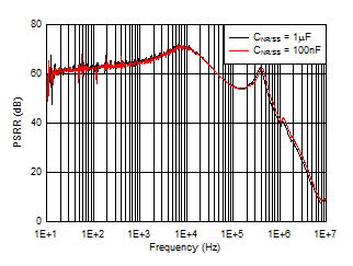
| VIN = –16 V, VOUT = –15 V, IOUT = 1 A, CFF = 10 nF, COUT = 2 × 10 µF |
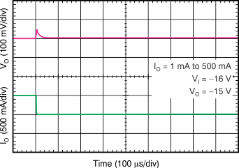 Figure 35. Load Transient
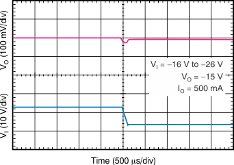 Figure 37. Line Transient
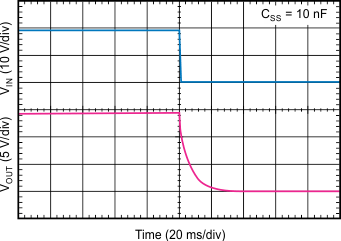 Figure 39. Capacitor-Programmable Soft-Start
| VIN = –16 V, VOUT = –15 V, IOUT = 1 A, CFF = 10 nF, COUT = 2 × µF |
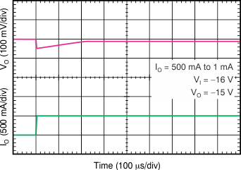 Figure 36. Load Transient
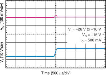 Figure 38. Line Transient
8.3 Do's and Don’ts
Place at least one low ESR 10-µF capacitor as close as possible to both the IN and OUT terminals of the regulator to the GND pin.
Provide adequate thermal paths away from the device.
Do not place the input or output capacitor more than 10 mm away from the regulator.
Do not exceed the absolute maximum ratings.
Do not float the EN pin.
Do not resistively or inductively load the NR/SS pin.
