SBVS169D December   2011  – April 2015 TPS7A33

PRODUCTION DATA.  

  1. Features
  2. Applications
  3. Description
  4. Revision History
  5. Pin Configuration and Functions
  6. Specifications
    1. 6.1 Absolute Maximum Ratings
    2. 6.2 ESD Ratings
    3. 6.3 Recommended Operating Conditions
    4. 6.4 Thermal Information
    5. 6.5 Electrical Characteristics
    6. 6.6 Typical Characteristics
  7. Detailed Description
    1. 7.1 Overview
    2. 7.2 Functional Block Diagram
    3. 7.3 Feature Description
      1. 7.3.1 Internal Current Limit
      2. 7.3.2 Enable Pin Operation
      3. 7.3.3 Programmable Soft-Start
      4. 7.3.4 Thermal Protection
    4. 7.4 Device Functional Modes
      1. 7.4.1 Normal Operation
      2. 7.4.2 Dropout Operation
      3. 7.4.3 Disabled
  8. Application and Implementation
    1. 8.1 Application Information
      1. 8.1.1  Adjustable Operation
      2. 8.1.2  Capacitor Recommendations
      3. 8.1.3  Input and Output Capacitor Requirements
      4. 8.1.4  Noise Reduction and Feed-Forward Capacitor Requirements
      5. 8.1.5  Post DC-DC Converter Filtering
      6. 8.1.6  Audio Applications
      7. 8.1.7  Maximum AC Performance
      8. 8.1.8  Power-Supply Rejection
      9. 8.1.9  Output Noise
      10. 8.1.10 Transient Response
      11. 8.1.11 Power for Precision Analog
    2. 8.2 Typical Application
      1. 8.2.1 Design Requirements
      2. 8.2.2 Detailed Design Procedure
      3. 8.2.3 Application Curves
    3. 8.3 Do's and Don’ts
  9. Power Supply Recommendations
  10. 10Layout
    1. 10.1 Layout Guidelines
      1. 10.1.1 Improve PSRR and Noise Performance
    2. 10.2 Layout Example
    3. 10.3 Thermal Performance and Heat Sink Selection
    4. 10.4 Package Mounting
  11. 11Device and Documentation Support
    1. 11.1 Device Support
      1. 11.1.1 Development Support
        1. 11.1.1.1 Evaluation Modules
        2. 11.1.1.2 Spice Models
      2. 11.1.2 Device Nomenclature
    2. 11.2 Documentation Support
      1. 11.2.1 Related Documentation
    3. 11.3 Trademarks
    4. 11.4 Electrostatic Discharge Caution
    5. 11.5 Glossary
  12. 12Mechanical, Packaging, and Orderable Information

Package Options

Mechanical Data (Package|Pins)
Thermal pad, mechanical data (Package|Pins)
Orderable Information

5 Pin Configuration and Functions

KC Package
7-Pin TO-220
Top View
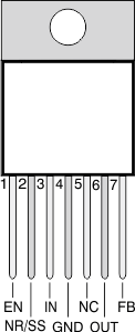
TPS7A33 po_7pin_bvs169.gif
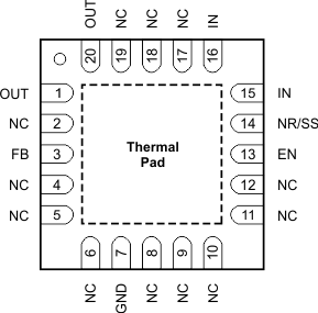
RGW Package
20-Pin VQFN
Top View
TPS7A33 po_20pin_bvs169.gif

Pin Functions

PIN I/O DESCRIPTION
NAME TO-220 VQFN
EN 1 13 I This pin turns the regulator on or off. If VEN ≥ VEN(+HI) or VEN ≤ VEN(–HI), the regulator is enabled.
If VEN(+LO) ≥ VEN ≥ VEN(–LO), the regulator is disabled. The EN pin can be connected to IN, if not used. |VEN| ≤ |VIN|.
FB 7 3 I This pin is the input to the control-loop error amplifier. It is used to set the output voltage of the device. TI recommends connecting a 10-nF capacitor from FB to OUT (as close to the device as possible) to maximize AC performance.
GND 4 7 Ground
IN 3 15, 16 I Input supply. A capacitor greater than or equal to 10 nF must be tied from this pin to ground to assure stability. It is recommended to connect a 10-µF capacitor from IN to GND (as close to the device as possible) to reduce circuit sensitivity to printed-circuit-board (PCB) layout, especially when long input traces or high source impedances are encountered.
NC 5 2, 4-6, 8-12, 17-19 This pin can be left open or tied to any voltage between GND and IN.
NR/SS 2 14 Noise reduction pin. A capacitor connected from this pin to GND controls the soft-start function and allows RMS noise to be reduced to very low levels. TI recommends connecting a 1-µF capacitor from NR/SS to GND (as close to the device as possible) to filter the noise generated by the internal bandgap and maximize ac performance.
OUT 6 1, 20 O Regulator output. A capacitor greater than or equal to 10 µF must be tied from this pin to ground to assure stability. TI recommends connecting a 47-µF ceramic capacitor from OUT to GND (as close to the device as possible) to maximize ac performance.
Thermal
Pad
Tab Connect the thermal pad to a large-area ground plane. The thermal pad is internally connected to GND. An external heatsink can be installed to provide additional thermal performance.