SBVS298B September   2017  – July 2018 TPS7A53-Q1

PRODUCTION DATA.  

  1. Features
  2. Applications
  3. Description
    1.     Device Images
      1.      Powering RF Components
      2.      Output Voltage Noise vs Frequency and Output Voltage
  4. Revision History
  5. Pin Configuration and Functions
    1.     Pin Functions
  6. Specifications
    1. 6.1 Absolute Maximum Ratings
    2. 6.2 ESD Ratings
    3. 6.3 Recommended Operating Conditions
    4. 6.4 Thermal Information
    5. 6.5 Electrical Characteristics
    6. 6.6 Typical Characteristics
  7. Detailed Description
    1. 7.1 Overview
    2. 7.2 Functional Block Diagram
    3. 7.3 Feature Description
      1. 7.3.1 Voltage Regulation Features
        1. 7.3.1.1 DC Regulation
        2. 7.3.1.2 AC and Transient Response
      2. 7.3.2 System Start-Up Features
        1. 7.3.2.1 Programmable Soft Start (NR/SS Pin)
        2. 7.3.2.2 Internal Sequencing
          1. 7.3.2.2.1 Enable (EN)
          2. 7.3.2.2.2 Undervoltage Lockout (UVLO) Control
          3. 7.3.2.2.3 Active Discharge
        3. 7.3.2.3 Power-Good Output (PG)
      3. 7.3.3 Internal Protection Features
        1. 7.3.3.1 Foldback Current Limit (ICL)
        2. 7.3.3.2 Thermal Protection (Tsd)
    4. 7.4 Device Functional Modes
      1. 7.4.1 Regulation
      2. 7.4.2 Disabled
      3. 7.4.3 Current Limit Operation
  8. Application and Implementation
    1. 8.1 Application Information
      1. 8.1.1  Recommended Capacitor Types
        1. 8.1.1.1 Input and Output Capacitor Requirements (CIN and COUT)
        2. 8.1.1.2 Noise-Reduction and Soft-Start Capacitor (CNR/SS)
        3. 8.1.1.3 Feed-Forward Capacitor (CFF)
      2. 8.1.2  Soft Start and Inrush Current
      3. 8.1.3  Optimizing Noise and PSRR
      4. 8.1.4  Charge Pump Noise
      5. 8.1.5  Current Sharing
      6. 8.1.6  Adjustable Operation
      7. 8.1.7  Power-Good Operation
      8. 8.1.8  Undervoltage Lockout (UVLO) Operation
      9. 8.1.9  Dropout Voltage (VDO)
      10. 8.1.10 Device Behavior During Transition From Dropout Into Regulation
      11. 8.1.11 Load Transient Response
      12. 8.1.12 Reverse Current Protection Considerations
      13. 8.1.13 Power Dissipation (PD)
      14. 8.1.14 Estimating Junction Temperature
    2. 8.2 Typical Application
      1. 8.2.1 Design Requirements
      2. 8.2.2 Detailed Design Procedure
      3. 8.2.3 Application Curves
  9. Power Supply Recommendations
  10. 10Layout
    1. 10.1 Layout Guidelines
      1. 10.1.1 Board Layout
      2. 10.1.2 RTK Package — High CTE Mold Compound
    2. 10.2 Layout Example
  11. 11Device and Documentation Support
    1. 11.1 Device Support
      1. 11.1.1 Development Support
        1. 11.1.1.1 Reference Designs
      2. 11.1.2 Device Nomenclature
    2. 11.2 Documentation Support
      1. 11.2.1 Related Documentation
    3. 11.3 Receiving Notification of Documentation Updates
    4. 11.4 Support Resources
    5. 11.5 Trademarks
    6. 11.6 Electrostatic Discharge Caution
    7. 11.7 Glossary
  12. 12Mechanical, Packaging, and Orderable Information

Package Options

Refer to the PDF data sheet for device specific package drawings

Mechanical Data (Package|Pins)
  • RGR|20
  • RTK|20
Thermal pad, mechanical data (Package|Pins)
Orderable Information

Typical Characteristics

at TA = 25°C, VIN = 1.4 V or VIN = VOUT(NOM) + 0.4 V (whichever is greater), VBIAS = open, VOUT(NOM) = 0.8 V, VEN = 1.1 V, COUT = 47 µF, CNR/SS = 0 nF, CFF = 0 nF, and PG pin pulled up to VIN with 100 kΩ (unless otherwise noted)
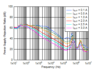
TPS7A53-Q1 PSRR_vs_Iout.gif
VIN = 1.1 V, VBIAS = 5 V,
COUT = 47 µF || 10 µF || 10 µF, CNR/SS = 10 nF, CFF = 10 nF
Figure 1. PSRR vs Frequency and IOUT
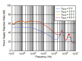
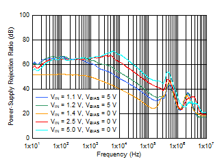
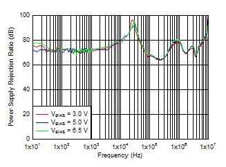
TPS7A53-Q1 PSRR_vs_Vbias.gif
VIN = 1.4 V, IOUT = 1 A,
COUT = 47 µF || 10 µF || 10 µF, CNR/SS = 10 nF, CFF = 10 nF
Figure 3. PSRR vs Frequency and VBIAS
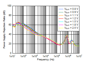
TPS7A53-Q1 PSRR_vs_Vout_with_Bias.gif
VIN = VOUT + 0.3 V, VBIAS = 5.0 V, IOUT = 3 A,
COUT = 47 µF || 10 µF || 10 µF, CNR/SS = 10 nF, CFF = 10 nF
Figure 5. PSRR vs Frequency and VOUT With Bias
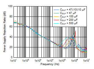
TPS7A53-Q1 PSRR_vs_Cout.gif
VIN = VOUT + 0.3 V, VOUT = 1 V, IOUT = 3 A, CNR/SS = 10 nF,
CFF = 10 nF
Figure 7. PSRR vs Frequency and COUT
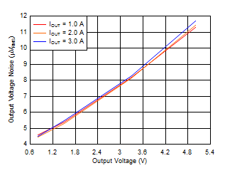
TPS7A53-Q1 Noise_vs_Iout_Vout.gif
VIN = VOUT + 0.3 V and VBIAS = 5 V for VOUT ≤ 2.2 V,
COUT = 47 µF || 10 µF || 10 µF, CNR/SS = 10 nF, CFF = 10 nF,
RMS noise BW = 10 Hz to 100 kHz
Figure 9. Output Voltage Noise vs Output Voltage
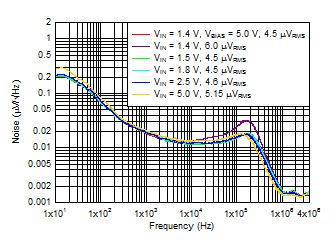
TPS7A53-Q1 Noise_vs_Vin.gif
IOUT = 3 A, COUT = 47 µF || 10 µF || 10 µF, CNR/SS = 10 nF,
CFF = 10 nF, RMS noise BW = 10 Hz to 100 kHz
Figure 11. Output Noise vs Frequency and VIN
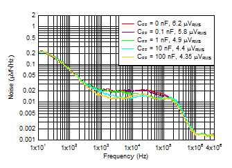
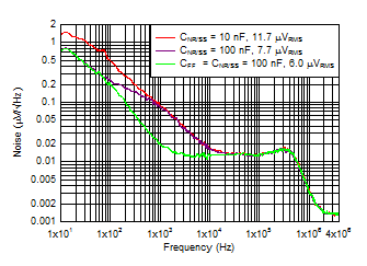
TPS7A53-Q1 Noise_vs_Cff.gif
VIN = VOUT + 0.3 V, VBIAS = 5 V, IOUT = 3 A, sequencing with a dc-dc converter and PG, COUT = 47 µF || 10 µF || 10 µF,
CNR/SS = 10 nF, RMS noise BW = 10 Hz to 100 kHz
Figure 13. Output Noise vs Frequency and CFF
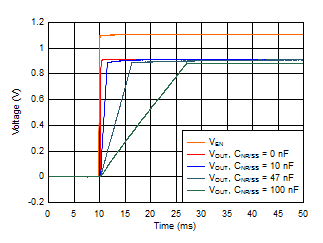
TPS7A53-Q1 Startup_Vs_Cnr.gif
VIN = 1.2 V, VOUT = 0.9 V, VBIAS = 5.0 V, IOUT = 3 A,
COUT = 47 µF || 10 µF || 10 µF, CFF = 10 nF
Figure 15. Start-Up Waveform vs Time and CNR/SS
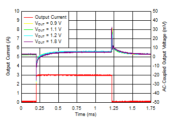
TPS7A53-Q1 Load_trans_vs_Vout_no_bias.gif
IOUT, DC = 100 mA, COUT = 47 µF || 10 µF || 10 µF,
CNR/SS = CFF = 10 nF, slew rate = 1 A/µs
Figure 17. Load Transient vs Time and VOUT Without Bias
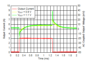
TPS7A53-Q1 Load_Trans_vs_preload.gif
VIN = 1.2 V, VBIAS = 5.0 V, COUT = 47 µF || 10 µF || 10 µF,
CNR/SS = CFF = 10 nF, slew rate = 1 A/µs
Figure 19. Load Transient vs Time and DC Load
(VOUT = 0.9 V)
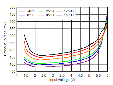
TPS7A53-Q1 D021-SBVS298-01.gif
IOUT = 3 A, VBIAS = 6.5 V
Figure 21. Dropout Voltage vs Input Voltage With Bias
TPS7A53-Q1 D023-SBVS298-01.gif
VIN = 1.1 V, VBIAS = 3 V
Figure 23. Dropout Voltage vs Output Current With Bias
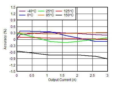
TPS7A53-Q1 D026-SBVS298-01.gif
VIN = 1.4 V, VBIAS = 0 V
Figure 25. Load Regulation With Bias
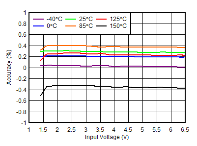
TPS7A53-Q1 D032-SBVS298-02.gif
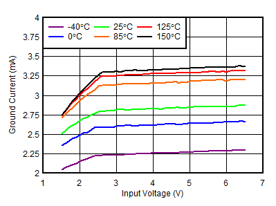
VBIAS = 0 V, IOUT = 5 mA
Figure 27. Quiescent Current vs Input Voltage
TPS7A53-Q1 D034-SBVS298-02.gif
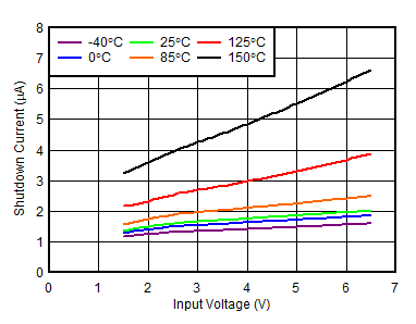
VBIAS = 0 V
Figure 29. Shutdown Current vs Input Voltage
TPS7A53-Q1 D036-SBVS298-01.gif
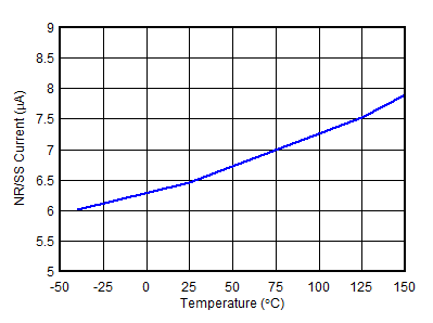
VBIAS = 0 V
Figure 31. NR/SS Current vs Temperature
TPS7A53-Q1 D038-SBVS298-02.gif
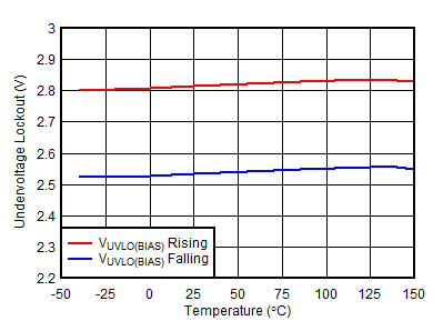
VIN = 1.1 V
Figure 33. VBIAS UVLO vs Temperature
TPS7A53-Q1 D040-SBVS298-02.gif
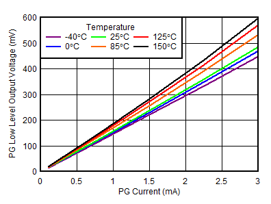
Figure 35. PG Voltage vs PG Current Sink
TPS7A53-Q1 D042-SBVS298-01.gif
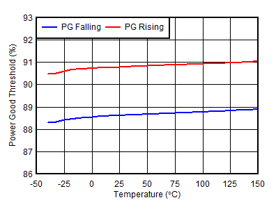
Figure 37. PG Threshold vs Temperature
TPS7A53-Q1 PSRR_vs_Vin_with_Bias.gif
IOUT = 3 A, VBIAS = 5 V,
COUT = 47 µF || 10 µF || 10 µF, CNR/SS = 10 nF, CFF = 10 nF
Figure 2. PSRR vs Frequency and VIN With Bias
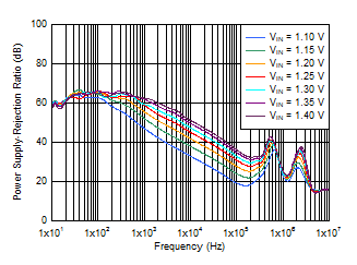
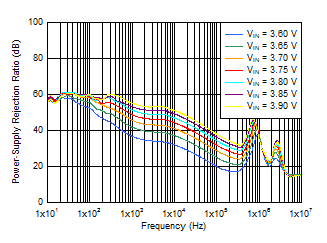
TPS7A53-Q1 PSRR_vs_VIN.gif
IOUT = 1 A,
COUT = 47 µF || 10 µF || 10 µF, CNR/SS = 10 nF, CFF = 10 nF
Figure 4. PSRR vs Frequency and VIN
TPS7A53-Q1 PSRR_vs_Vin_3p3Vout.gif
IOUT = 3 A, COUT = 47 µF || 10 µF || 10 µF, CNR/SS = 10 nF,
CFF = 10 nF
Figure 6. PSRR vs Frequency and VIN for VOUT = 3.3 V
TPS7A53-Q1 7a84_Bias_PSRR.gif
VIN = VOUT + 0.3 V, VOUT = 1 V, IOUT = 3 A,
COUT = 47 µF || 10 µF || 10 µF, CNR/SS = 10 nF, CFF = 10 nF
Figure 8. VBIAS PSRR vs Frequency and VBIAS
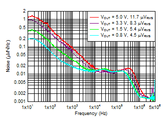
TPS7A53-Q1 Noise_vs_Vout.gif
VIN = VOUT + 0.3 V and VBIAS = 5 V for VOUT ≤ 2.2 V, IOUT = 3 A, COUT = 47 µF || 10 µF || 10 µF, CNR/SS = 10 nF, CFF = 10 nF,
RMS noise BW = 10 Hz to 100 kHz
Figure 10. Output Noise vs Frequency and VOUT
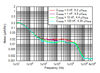
TPS7A53-Q1 Noise_vs_Cnr.gif
VIN = VOUT + 0.3 V, VBIAS = 5 V, IOUT = 3 A, COUT = 47 µF ||
10 µF || 10 µF, CFF = 10 nF, RMS noise BW = 10 Hz to 100 kHz
Figure 12. Output Noise vs Frequency and CNR/SS
TPS7A53-Q1 Noise_vs_Cnr_5Vout.gif
IOUT = 3 A, COUT = 47 µF || 10 µF || 10 µF, CFF = 10 nF,
RMS noise BW = 10 Hz to 100 kHz
Figure 14. Output Noise at 5.0-V Output
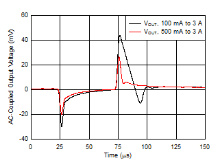
TPS7A53-Q1 Load_trans_vs_Vout.gif
VIN = VOUT + 0.3 V, VBIAS = 5 V, IOUT, DC = 100 mA, slew rate = 1 A/µs, CNR/SS = CFF = 10 nF, COUT = 47 µF || 10 µF || 10 µF
Figure 16. Load Transient vs Time and VOUT With Bias
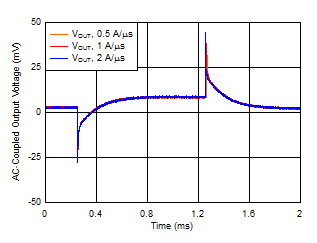
TPS7A53-Q1 Load_trans_vs_SR.gif
VOUT = 5 V, IOUT, DC = 100 mA, IOUT = 100 mA to 3 A,
COUT = 47 µF || 10 µF || 10 µF, CNR/SS = CFF = 10 nF
Figure 18. Load Transient vs Time and Slew Rate
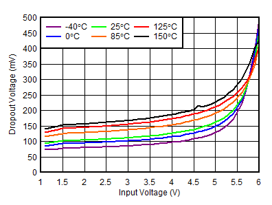
TPS7A53-Q1 D020-SBVS298-02.gif
IOUT = 3 A, VBIAS = 0 V
Figure 20. Dropout Voltage vs Input Voltage Without Bias
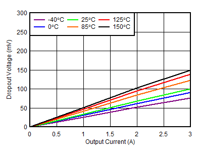
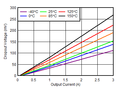
TPS7A53-Q1 D022-SBVS298-01.gif
VIN = 1.4 V, VBIAS = 0 V
Figure 22. Dropout Voltage vs Output Current Without Bias
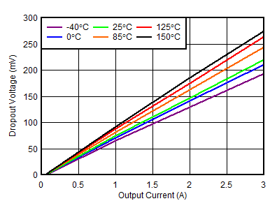
TPS7A53-Q1 D024-SBVS298-01.gif
VIN = 5.5 V
Figure 24. Dropout Voltage vs Output Current (High VIN)
TPS7A53-Q1 D029-SBVS298-01.gif
VOUT = 0.8 V, VBIAS = 0 V, IOUT = 5 mA
Figure 26. Line Regulation Without Bias
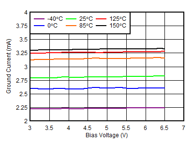
TPS7A53-Q1 D033-SBVS298-01.gif
VIN = 1.1 V, IOUT = 5 mA
Figure 28. Quiescent Current vs Bias Voltage
TPS7A53-Q1 D035-SBVS298-01.gif
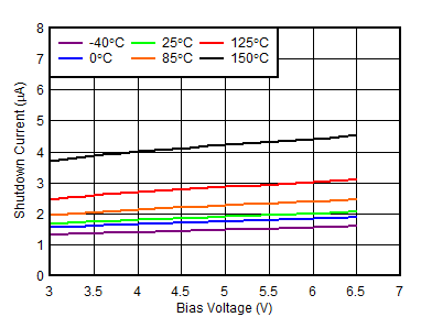
VIN = 1.1 V
Figure 30. Shutdown Current vs Bias Voltage
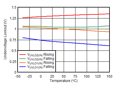
TPS7A53-Q1 D037-SBVS298-02.gif
Figure 32. VIN UVLO vs Temperature
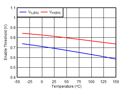
TPS7A53-Q1 D039-SBVS298-01.gif
VIN = 1.4 V, 6.5 V
Figure 34. Enable Threshold vs Temperature
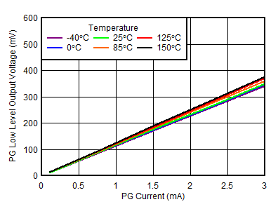
TPS7A53-Q1 D041-SBVS298-01.gif
VIN = 6.5 V
Figure 36. PG Voltage vs PG Current Sink
TPS7A53-Q1 D043-SBVS298-01.gif
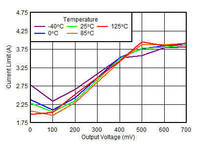
Temperature limited because of power dissipation
Figure 38. Foldback Current Limit vs Output Voltage