SLVSA62J March   2010  – March 2020 TPS7A60-Q1 , TPS7A61-Q1

PRODUCTION DATA.  

  1. Features
  2. Applications
  3. Description
    1.     Device Images
      1.      Programmable Reset Delay Option
      2.      Enable Option
  4. Revision History
  5. Device Comparison Table
  6. Pin Configuration and Functions
    1.     Pin Functions
  7. Specifications
    1. 7.1 Absolute Maximum Ratings
    2. 7.2 ESD Ratings
    3. 7.3 Recommended Operating Conditions
    4. 7.4 Thermal Information
    5. 7.5 Electrical Characteristics
    6. 7.6 Switching Characteristics
    7. 7.7 Typical Characteristics
  8. Detailed Description
    1. 8.1 Overview
    2. 8.2 Functional Block Diagrams
    3. 8.3 Feature Description
      1. 8.3.1 Reset Delay and Reset Output
      2. 8.3.2 Charge Pump Operation
      3. 8.3.3 Undervoltage Shutdown
      4. 8.3.4 Low-Voltage Tracking
      5. 8.3.5 Integrated Fault Protection
      6. 8.3.6 Thermal Shutdown
    4. 8.4 Device Functional Modes
      1. 8.4.1 Low-Power Mode
      2. 8.4.2 Sleep Mode (TPS7A61-Q1 Only)
      3. 8.4.3 Regulation Mode
  9. Application and Implementation
    1. 9.1 Application Information
    2. 9.2 Typical Applications
      1. 9.2.1 TPS7A60-Q1 Typical Application
        1. 9.2.1.1 Design Requirements
        2. 9.2.1.2 Detailed Design Procedure
          1. 9.2.1.2.1 Input Capacitor
          2. 9.2.1.2.2 Output Capacitor
        3. 9.2.1.3 Application Curve
      2. 9.2.2 TPS7A61-Q1 Typical Application
        1. 9.2.2.1 Design Requirements
        2. 9.2.2.2 Detailed Design Procedure
        3. 9.2.2.3 Application Curve
  10. 10Power Supply Recommendations
  11. 11Layout
    1. 11.1 Layout Guidelines
      1. 11.1.1 Power Dissipation and Thermal Considerations
    2. 11.2 Layout Examples
  12. 12Device and Documentation Support
    1. 12.1 Related Links
    2. 12.2 Receiving Notification of Documentation Updates
    3. 12.3 Community Resources
    4. 12.4 Trademarks
    5. 12.5 Electrostatic Discharge Caution
    6. 12.6 Glossary
  13. 13Mechanical, Packaging, and Orderable Information

Package Options

Mechanical Data (Package|Pins)
Thermal pad, mechanical data (Package|Pins)
Orderable Information

Thermal Shutdown

These devices incorporate a thermal shutdown (TSD) circuit as a protection from overheating. For continuous normal operation, the junction temperature should not exceed the TSD trip point. If the junction temperature exceeds the TSD trip point, the output is turned off. When the junction temperature falls below the TSD trip point, the output is turned on again. This is shown in Figure 21.
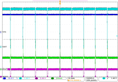
TPS7A60-Q1 TPS7A61-Q1 thermal_shutdown_wave_lvsa62.gif
VIN = 24 V IOUT = 300 mA VOUT = 5 V
Figure 21. Thermal Cycling Waveform for the TPS7A6150-Q1