SLVSA62J March   2010  – March 2020 TPS7A60-Q1 , TPS7A61-Q1

PRODUCTION DATA.  

  1. Features
  2. Applications
  3. Description
    1.     Device Images
      1.      Programmable Reset Delay Option
      2.      Enable Option
  4. Revision History
  5. Device Comparison Table
  6. Pin Configuration and Functions
    1.     Pin Functions
  7. Specifications
    1. 7.1 Absolute Maximum Ratings
    2. 7.2 ESD Ratings
    3. 7.3 Recommended Operating Conditions
    4. 7.4 Thermal Information
    5. 7.5 Electrical Characteristics
    6. 7.6 Switching Characteristics
    7. 7.7 Typical Characteristics
  8. Detailed Description
    1. 8.1 Overview
    2. 8.2 Functional Block Diagrams
    3. 8.3 Feature Description
      1. 8.3.1 Reset Delay and Reset Output
      2. 8.3.2 Charge Pump Operation
      3. 8.3.3 Undervoltage Shutdown
      4. 8.3.4 Low-Voltage Tracking
      5. 8.3.5 Integrated Fault Protection
      6. 8.3.6 Thermal Shutdown
    4. 8.4 Device Functional Modes
      1. 8.4.1 Low-Power Mode
      2. 8.4.2 Sleep Mode (TPS7A61-Q1 Only)
      3. 8.4.3 Regulation Mode
  9. Application and Implementation
    1. 9.1 Application Information
    2. 9.2 Typical Applications
      1. 9.2.1 TPS7A60-Q1 Typical Application
        1. 9.2.1.1 Design Requirements
        2. 9.2.1.2 Detailed Design Procedure
          1. 9.2.1.2.1 Input Capacitor
          2. 9.2.1.2.2 Output Capacitor
        3. 9.2.1.3 Application Curve
      2. 9.2.2 TPS7A61-Q1 Typical Application
        1. 9.2.2.1 Design Requirements
        2. 9.2.2.2 Detailed Design Procedure
        3. 9.2.2.3 Application Curve
  10. 10Power Supply Recommendations
  11. 11Layout
    1. 11.1 Layout Guidelines
      1. 11.1.1 Power Dissipation and Thermal Considerations
    2. 11.2 Layout Examples
  12. 12Device and Documentation Support
    1. 12.1 Related Links
    2. 12.2 Receiving Notification of Documentation Updates
    3. 12.3 Community Resources
    4. 12.4 Trademarks
    5. 12.5 Electrostatic Discharge Caution
    6. 12.6 Glossary
  13. 13Mechanical, Packaging, and Orderable Information

Package Options

Mechanical Data (Package|Pins)
Thermal pad, mechanical data (Package|Pins)
Orderable Information

Typical Characteristics

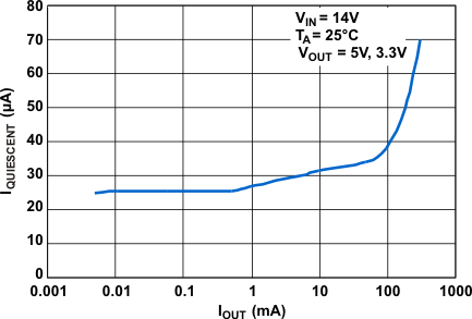
TPS7A60-Q1 TPS7A61-Q1 g_iq_iout_lvsa62.gif
Figure 1. Quiescent Current vs Load Current
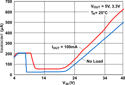
TPS7A60-Q1 TPS7A61-Q1 g_iq_vin_lvsa62.gif
Figure 3. Quiescent Current vs Input Voltage
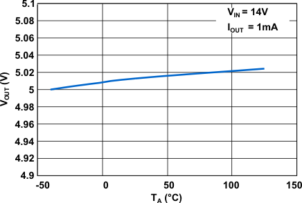
TPS7A60-Q1 TPS7A61-Q1 g_vout_ta_lvsa62.gif
Figure 5. Output Voltage vs Ambient Air Temperature
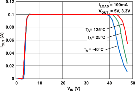
TPS7A60-Q1 TPS7A61-Q1 g_iout_vin_lvsa62.gif
Figure 7. Output Voltage vs Input Voltage
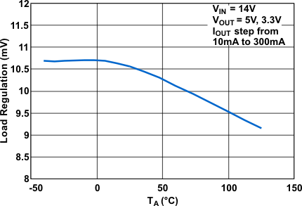
TPS7A60-Q1 TPS7A61-Q1 g_loadreg_ta_lvsa62.gif
Figure 9. Load Regulation vs Ambient Air Temperature
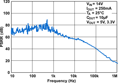
TPS7A60-Q1 TPS7A61-Q1 g_psrr_heavy_lvsa62.gif
Figure 11. PSRR at Heavy Load Current
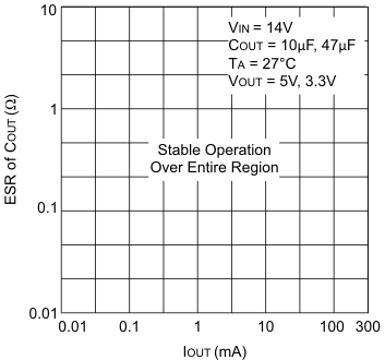
TPS7A60-Q1 TPS7A61-Q1 g_esr_iout_page1_lvsa62.gif
Figure 13. ESR Stability vs Load Current
for TPS7A60-Q1 and TPS7A61-Q1
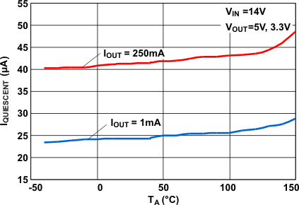
TPS7A60-Q1 TPS7A61-Q1 g_iq_ta_lvsa62.gif
Figure 2. Quiescent Current vs Ambient Air Temperature
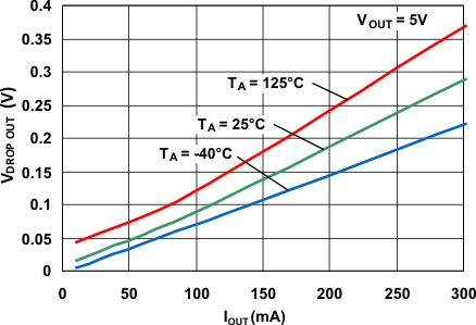
TPS7A60-Q1 TPS7A61-Q1 g_vdo_iout_lvsa62.gif
Figure 4. Dropout Voltage (1) vs Load Current
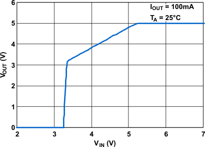
TPS7A60-Q1 TPS7A61-Q1 g_vout_vin_lvsa62.gif
Figure 6. Output Voltage vs Input Voltage
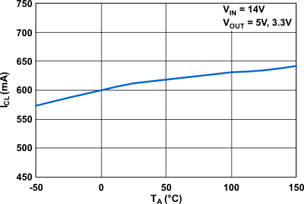
TPS7A60-Q1 TPS7A61-Q1 g_icl_ta_lvsa62.gif
Figure 8. Output Current Limit vs Ambient Air Temperature
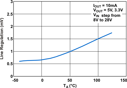
TPS7A60-Q1 TPS7A61-Q1 g_linereg_ta_lvsa62.gif
Figure 10. Line Regulation vs Ambient Air Temperature
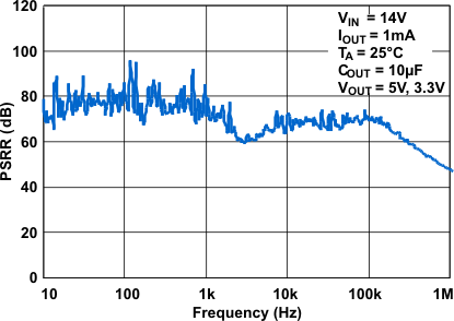
TPS7A60-Q1 TPS7A61-Q1 g_psrr_light_lvsa62.gif
Figure 12. PSRR at Light Load Current
Dropout voltage is measured when the output voltage drops by 100 mV from the regulated output voltage level. (For example, dropout voltage for the TPS7A6050-Q1 is measured when the output voltage drops down to 4.9 V from 5 V.)