SLVSD64 December 2015 TPS7A6650H-Q1
PRODUCTION DATA.
- 1 Features
- 2 Applications
- 3 Description
- 4 Revision History
- 5 Pin Configuration and Functions
- 6 Specifications
- 7 Detailed Description
- 8 Application and Implementation
- 9 Power Supply Recommendations
- 10Layout
- 11Device and Documentation Support
- 12Mechanical, Packaging, and Orderable Information
Package Options
Mechanical Data (Package|Pins)
- DGN|8
Thermal pad, mechanical data (Package|Pins)
- DGN|8
Orderable Information
6 Specifications
6.1 Absolute Maximum Ratings
over operating ambient temperature range (unless otherwise noted) (1)| MIN | MAX | UNIT | ||
|---|---|---|---|---|
| Vin, EN | Unregulated input(2) (3) | –0.3 | 45 | V |
| Vout | Regulated output | –0.3 | 7 | V |
| CT | –0.3 | 25 | V | |
| PG | –0.3 | Vout | V | |
| TJ | Operating junction temperature range | –40 | 160 | °C |
| Tstg | Storage temperature range | –65 | 160 | °C |
(1) Stresses beyond those listed under Absolute Maximum Ratings may cause permanent damage to the device. These are stress ratings only, and do not imply functional operation of the device at these or any other conditions beyond those indicated under Recommended Operating Conditions. Exposure to absolute-maximum-rated conditions for extended periods may affect device reliability.
(2) All voltage values are with respect to GND
(3) Absolute maximum voltage, withstand 45 V for 200 ms
6.2 ESD Ratings
| VALUE | UNIT | ||||
|---|---|---|---|---|---|
| V(ESD) | Electrostatic discharge | Human body model (HBM), per AEC Q100-002(1) | ±4000 | V | |
| Charged device model (CDM), per AEC Q100-011 | All pins | ±1000 | |||
| Corner pins (1, 4, 5, and 8) | ±1000 | ||||
(1) AEC Q100-002 indicates HBM stressing is done in accordance with the ANSI/ESDA/JEDEC JS-001 specification.
spacer
6.3 Recommended Operating Conditions
over operating ambient temperature range (unless otherwise noted)| MIN | MAX | UNIT | ||
|---|---|---|---|---|
| Vin | Unregulated input | 4 | 40 | V |
| EN | 0 | 40 | V | |
| CT | 0 | 20 | V | |
| Vout | 1.5 | 5.5 | V | |
| PG | Low voltage (I/O) | 0 | 5.5 | V |
| TA | Operating ambient temperature | –40 | 150 | °C |
6.4 Thermal Information
| THERMAL METRIC(1) | TPS7A6650H-Q1 | UNIT | |
|---|---|---|---|
| DGN (HVSSOP) | |||
| 8 PINS | |||
| RθJA | Junction-to-ambient thermal resistance | 63.4 | °C/W |
| RθJC(top) | Junction-to-case (top) thermal resistance | 53 | °C/W |
| RθJB | Junction-to-board thermal resistance(2) | 37.4 | °C/W |
| ψJT | Junction-to-top characterization parameter | 3.7 | °C/W |
| ψJB | Junction-to-board characterization parameter | 37.1 | °C/W |
| RθJC(bot) | Junction-to-case (bottom) thermal resistance | 13.5 | °C/W |
(1) For more information about traditional and new thermal metrics, see the Semiconductor and IC Package Thermal Metrics application report (SPRA953).
(2) The junction-to-board thermal resistance is obtained by simulating in an environment with a ring cold plate fixture to control the PCB temperature, as described in JESD51-8.
6.5 Electrical Characteristics
V(Vin) = 14 V, 1 mΩ < ESR < 2 Ω, TJ = –40°C to 160°C (unless otherwise noted)| PARAMETER | TEST CONDITIONS | MIN | TYP | MAX | UNIT | |
|---|---|---|---|---|---|---|
| SUPPLY VOLTAGE AND CURRENT (Vin) | ||||||
| V(Vin) | Input voltage | IO = 1 mA | 5.5 | 40 | V | |
| I(q) | Quiescent current | V(Vin) = 5.5 V to 40 V, EN = ON, IO = 0.2 mA | 12 | 22 | µA | |
| I(Sleep) | Input sleep current | No load current and EN = OFF | 4 | µA | ||
| I(EN) | EN pin current | V(EN) = 40 V | 1 | µA | ||
| V(VinUVLO) | Undervoltage detection | Ramp V(Vin) down until output turns OFF | 2.6 | V | ||
| V(UVLOhys) | Undervoltage hysteresis | 1 | V | |||
| ENABLE INPUT (EN) | ||||||
| VIL | Logic input low level | 0 | 0.4 | V | ||
| VIH | Logic input high level | 1.7 | V | |||
| REGULATED OUTPUT (Vout) | ||||||
| V(Vout) | Regulated output | IO = 1 mA, TJ = 25°C | –1% | 1% | ||
| V(Vin) = 6 V to 40 V, IO = 1 mA to 50 mA | –2% | 2% | ||||
| V(line-reg) | Line regulation | V(Vin) = 5.5 V to 40 V, IO = 50 mA | 5 | mV | ||
| V(load-reg) | Load regulation | IO = 1 mA to 50 mA | 20 | mV | ||
| V(dropout) | Dropout voltage | V(dropout) = V(Vin) – V(Vout), IOUT = 50 mA | 130 | 240 | mV | |
| IO | Output current | V(Vout) in regulation | 0 | 50 | mA | |
| I(lreg-CL) | Output current limit | V(Vout) short to ground | 500 | 800 | mA | |
| PSRR | Power supply ripple rejection(1) | V(Vin) = 12 V, IL = 10 mA, output capacitance = 2.2 µF, | ||||
| V(Vin) = 12 V, IL = 10 mA, output capacitance = 2.2 µF, frequency = 100 Hz | 60 | dB | ||||
| V(Vin) = 12 V, IL = 10 mA, output capacitance = 2.2 µF, frequency = 100 kHz | 40 | dB | ||||
| RESET (PG) | ||||||
| VOL | Reset output, low voltage | IOL = 0.5 mA | 0.4 | V | ||
| Ilkg | Leakage current | Reset pulled Vout through 10-kΩ resistor | 1 | µA | ||
| V(TH-POR) | Power-on-reset threshold | V(Vout) increasing | 89.6 | 91.6 | 93.6 | % of Vout |
| V(Thres) | Hysteresis | 2 | % of Vout | |||
| RESET DELAY (CT) | ||||||
| I(Chg) | Delay-capacitor charging current | V(CT) = 0 V | 1.4 | µA | ||
| V(th) | Threshold to release PG high | 1 | V | |||
| OPERATING TEMPERATURE RANGE | ||||||
| TJ | Junction temperature | –40 | 160 | °C | ||
| T(shutdown) | Junction shutdown temperature | 175 | °C | |||
| T(hyst) | Hysteresis of thermal shutdown | 20 | °C | |||
(1) Design information – Not tested
6.6 Switching Characteristics
over operating free-air temperature range (unless otherwise noted)| PARAMETER | TEST CONDITIONS | MIN | TYP | MAX | UNIT | |
|---|---|---|---|---|---|---|
| TIMING FOR RESET (PG) | ||||||
| t(POR) | Power-on-reset delay | Where C = delay capacitor value; capacitance C = 100 nF(1) | 50 | 100 | 180 | ms |
| t(POR-fixed) | No capacitor on pin | 100 | 290 | 650 | µs | |
| t(Deglitch) | Reset deglitch time | 20 | 250 | µs | ||
(1) This information only is not tested in production and equation basis is (C × 1) / 1 × 10–6 = td (delay time).
Where C = Delay capacitor value. Capacitance C range = 100 pF to 100 nF.
Where C = Delay capacitor value. Capacitance C range = 100 pF to 100 nF.
6.7 Qualification Summary
The TPS7A6650H-Q1 device has passed all the Grade 0 level qualification items required in AEC-Q100 with one exception: High temperature storage lifetime (HTSL). For the HTSL item, the Grade 0 level requirement is passing 175ºC for 1000 hours of stress. For this device, it passed at 160°C for 1000 hours stress.
6.8 Typical Characteristics
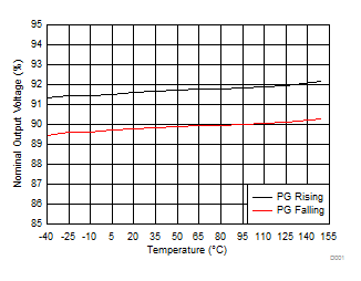
| Vin = 14 V | No Load |
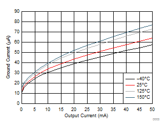
| Vin = 14 V |
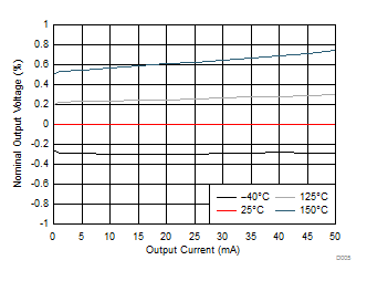
| Vin = 14 V |
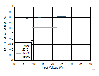
| Vin = 14 V | IL = 1 mA |
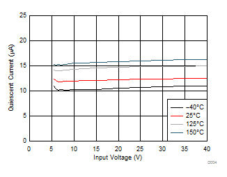
| IL = 0 |
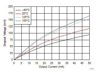
| Vin = 4 V |
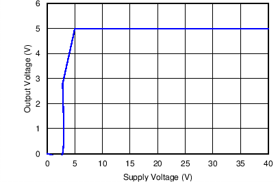 Figure 7. Output Voltage vs Supply Voltage (Fixed 5-V Version, IL = 0)
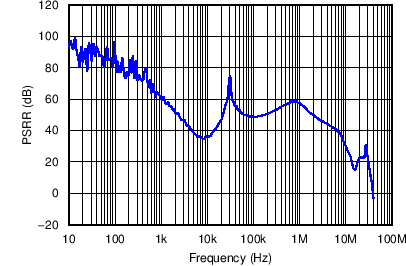 Figure 9. Power-Supply Rejection Ratio vs Frequency
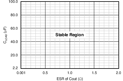 Figure 8. Load Capacitance vs ESR Stability
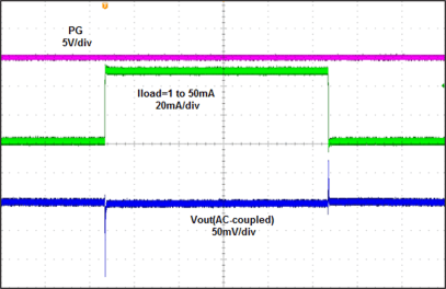 Figure 10. Load Transient Response, 10 ms/div
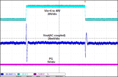 Figure 12. Line Transient Response, IL = 10 mA, 1 V/µs
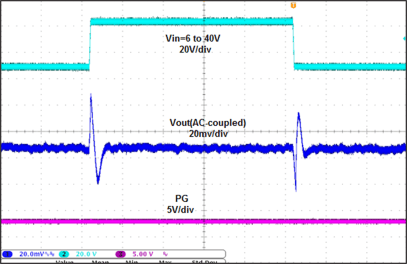 Figure 11. Line Transient Response, IL = 1 mA, 1 V/µs