SLVSBL0F December   2012  – December 2017 TPS7A66-Q1 , TPS7A69-Q1

PRODUCTION DATA.  

  1. Features
  2. Applications
  3. Description
    1.     Device Images
      1.      Hardware-Enable Option
      2.      Input-Voltage-Sensing Option
  4. Revision History
  5. Pin Configuration and Functions
    1.     Pin Functions
  6. Specifications
    1. 6.1 Absolute Maximum Ratings
    2. 6.2 ESD Ratings
    3. 6.3 Recommended Operating Conditions
    4. 6.4 Thermal Information
    5. 6.5 Electrical Characteristics
    6. 6.6 Switching Characteristics
    7. 6.7 Typical Characteristics
  7. Detailed Description
    1. 7.1 Overview
    2. 7.2 Functional Block Diagrams
    3. 7.3 Feature Description
      1. 7.3.1 Enable (EN)
      2. 7.3.2 Regulated Output (VOUT)
      3. 7.3.3 Power-On Reset (PG)
      4. 7.3.4 Reset Delay Timer (CT)
      5. 7.3.5 Sense Comparator (SI and SO for TPS7A69-Q1)
      6. 7.3.6 Adjustable Output Voltage (FB for TPS7A6601-Q1)
      7. 7.3.7 Undervoltage Shutdown
      8. 7.3.8 Low-Voltage Tracking
      9. 7.3.9 Thermal Shutdown
    4. 7.4 Device Functional Modes
      1. 7.4.1 Regulation
      2. 7.4.2 Disabled
      3. 7.4.3 Operation With V(VinUVLO)< VIN < VIN(min)
  8. Application and Implementation
    1. 8.1 Application Information
    2. 8.2 Typical Applications
      1. 8.2.1 TPS7A66-Q1 Typical Application
        1. 8.2.1.1 Design Requirements
        2. 8.2.1.2 Detailed Design Procedure
          1. 8.2.1.2.1 Input Capacitor
          2. 8.2.1.2.2 Output Capacitor
        3. 8.2.1.3 Application Curve
      2. 8.2.2 TPS7A69-Q1 Typical Application
        1. 8.2.2.1 Design Requirements
        2. 8.2.2.2 Detailed Design Procedure
          1. 8.2.2.2.1 Low-Voltage Tracking Threshold
        3. 8.2.2.3 Application Curve
  9. Power Supply Recommendations
  10. 10Layout
    1. 10.1 Layout Guidelines
      1. 10.1.1 Package Mounting
      2. 10.1.2 Board Layout Recommendations to Improve PSRR and Noise Performance
    2. 10.2 Layout Examples
    3. 10.3 Power Dissipation and Thermal Considerations
  11. 11Device and Documentation Support
    1. 11.1 Related Links
    2. 11.2 Receiving Notification of Documentation Updates
    3. 11.3 Community Resources
    4. 11.4 Trademarks
    5. 11.5 Electrostatic Discharge Caution
    6. 11.6 Glossary
  12. 12Mechanical, Packaging, and Orderable Information

Package Options

Mechanical Data (Package|Pins)
Thermal pad, mechanical data (Package|Pins)
Orderable Information

Typical Characteristics

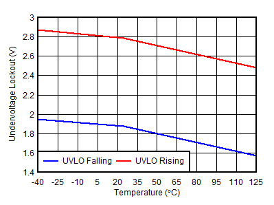
TPS7A66-Q1 TPS7A69-Q1 UVLO-01.gif
Figure 1. UVLO Thresholds vs Temperature
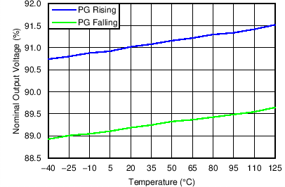
TPS7A66-Q1 TPS7A69-Q1 C001_SLVSBL0.png
Figure 3. Power-Good Threshold Voltage vs Temperature (VIN = 14 V, No Load)
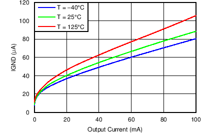
TPS7A66-Q1 TPS7A69-Q1 C003_SLVSBL0.png
Figure 5. Ground Current vs Output Current (VIN = 14 V)
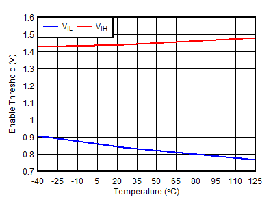
TPS7A66-Q1 TPS7A69-Q1 Ven Thresh-01.gif
Figure 2. Enable Thresholds vs Temperature
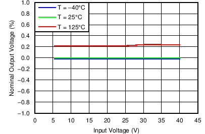
TPS7A66-Q1 TPS7A69-Q1 C002_SLVSBL0.png
Figure 4. Line Regulation (VIN = 14 V, IL = 1 mA)
TPS7A66-Q1 TPS7A69-Q1 C004_SLVSBL0.png
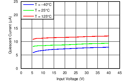
Figure 6. Quiescent Current vs Input Voltage (IL = 0)
TPS7A66-Q1 TPS7A69-Q1 C005_SLVSBL0.png
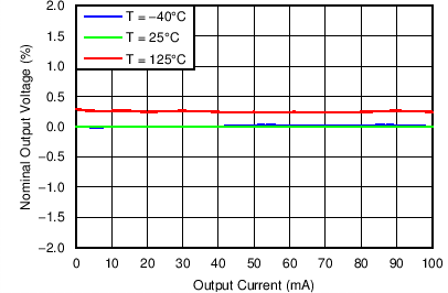
Figure 7. Load Regulation (VIN = 14 V)
TPS7A66-Q1 TPS7A69-Q1 C007_SLVSBL0.png
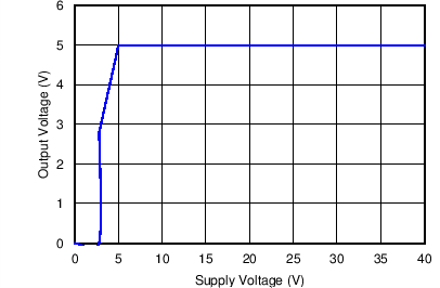
Figure 9. Output Voltage vs Supply Voltage
(Fixed 5-V Version, IL = 0)
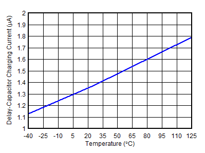
TPS7A66-Q1 TPS7A69-Q1 Ict-01.gif
Figure 11. CT Charging Current (VCT = 0)
TPS7A66-Q1 TPS7A69-Q1 C009_SLVSBL0.png
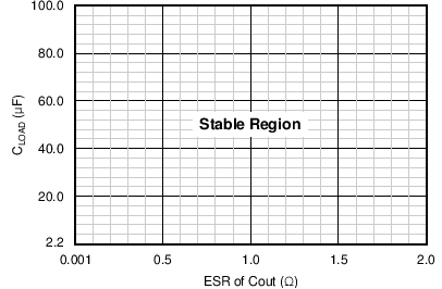
Figure 13. Load Capacitance vs ESR Stability
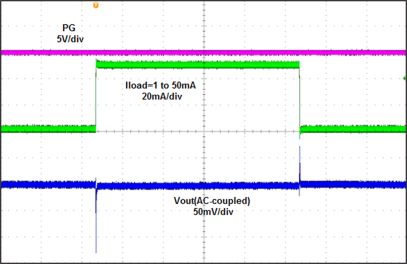
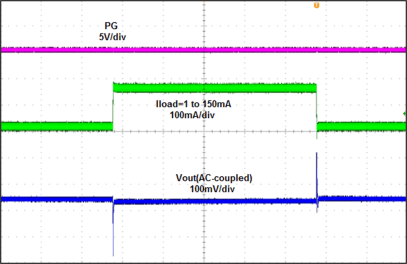
TPS7A66-Q1 TPS7A69-Q1 Scope-02_SLVSBL0.gif
All oscilloscope waveforms were taken at room temperature.
Figure 15. Load Transient Response, 10 ms/div
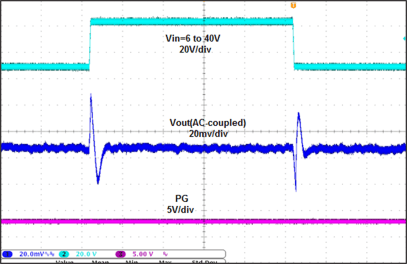
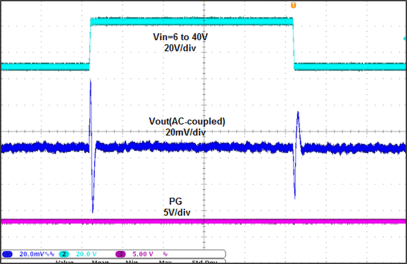
TPS7A66-Q1 TPS7A69-Q1 Scope-04_SLVSBL0.gif
All oscilloscope waveforms were taken at room temperature.
Figure 17. Line Transient Response, IL = 1 mA, 1 V/µs
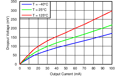
TPS7A66-Q1 TPS7A69-Q1 C006_SLVSBL0.png
Figure 8. Dropout Voltage vs Output Current (VIN = 4 V)
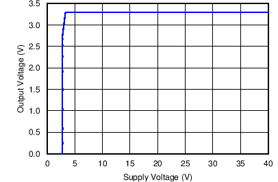
TPS7A66-Q1 TPS7A69-Q1 C008_SLVSBL0.png
Figure 10. Output Voltage vs Supply Voltage
(Fixed 3.3-V Version, IL = 0)
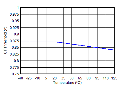
TPS7A66-Q1 TPS7A69-Q1 Vct-01.gif
Figure 12. CT Charging Threshold
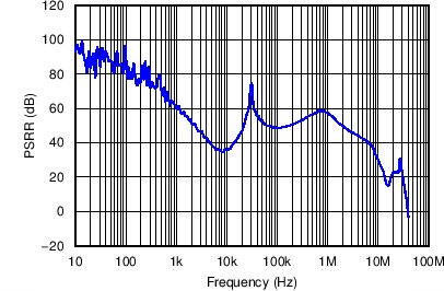
TPS7A66-Q1 TPS7A69-Q1 C010_SLVSBL0.png
Figure 14. Power-Supply Rejection Ratio vs Frequency
TPS7A66-Q1 TPS7A69-Q1 Scope-03_SLVSBL0.gif
All oscilloscope waveforms were taken at room temperature.
Figure 16. Load Transient Response, 10 ms/div
TPS7A66-Q1 TPS7A69-Q1 Scope-05_SLVSBL0.gif
All oscilloscope waveforms were taken at room temperature.
Figure 18. Line Transient Response, IL = 10 mA, 1 V/µs