SBVS248A November 2015 – November 2015 TPS7A88
PRODUCTION DATA.
- 1 Features
- 2 Applications
- 3 Description
- 4 Revision History
- 5 Pin Configuration and Functions
- 6 Specifications
-
7 Detailed Description
- 7.1 Overview
- 7.2 Functional Block Diagram
- 7.3 Feature Description
- 7.4 Device Functional Modes
- 8 Application and Implementation
- 9 Power Supply Recommendations
- 10Layout
- 11Device and Documentation Support
- 12Mechanical, Packaging, and Orderable Information
Package Options
Mechanical Data (Package|Pins)
- RTJ|20
Thermal pad, mechanical data (Package|Pins)
- RTJ|20
Orderable Information
8 Application and Implementation
NOTE
Information in the following applications sections is not part of the TI component specification, and TI does not warrant its accuracy or completeness. TI’s customers are responsible for determining suitability of components for their purposes. Customers should validate and test their design implementation to confirm system functionality.
8.1 Application Information
The TPS7A88 is a linear voltage regulator operating from 1.4 V to 6.5 V on the input and regulates voltages between 0.8 V to 5.0 V within 1% accuracy and a 1-A maximum output current. Efficiency is defined by the ratio of output voltage to input voltage because the TPS7A88 is a linear voltage regulator. To achieve high efficiency, the dropout voltage (VINx – VOUTx) must be as small as possible, thus requiring a very low dropout LDO. Successfully implementing an LDO in an application depends on the application requirements. This section discusses key device features and how to best implement them to achieve a reliable design.
8.1.1 Adjustable Outputs
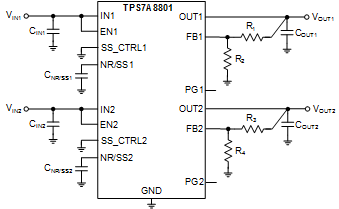
The output voltages of the TPS7A8801 can be adjusted from 0.8 V to 5.0 V by using resistor divider networks as shown in Figure 42.
 Figure 42. Adjustable Operation
R1, R3 and R2, R4 can be calculated for any output voltage range using Equation 2. This resistive network must provide a current equal to or greater than 5 μA for optimum noise performance.

If greater voltage accuracy is required, take into account the output voltage offset contributions resulting from the feedback pin current (IFB) and use 0.1% tolerance resistors.
Table 2 shows the resistor combination required to achieve a few of the most common rails using commercially-available, 0.1%-tolerance resistors to maximize nominal voltage accuracy and also abiding to the formula given in Equation 2.
Table 2. Recommended Feedback-Resistor Values
| VOUTx(TARGET)
(V) |
FEEDBACK RESISTOR VALUES(1) | |
|---|---|---|
| R1, R3 (kΩ) | R2, R4 (kΩ) | |
| 0.8 | Short | Open |
| 1.00 | 2.55 | 10.2 |
| 1.20 | 5.9 | 11.8 |
| 1.50 | 9.31 | 10.7 |
| 1.80 | 1.87 | 1.5 |
| 1.90 | 15.8 | 11.5 |
| 2.50 | 2.43 | 1.15 |
| 3.00 | 3.16 | 1.15 |
| 3.30 | 3.57 | 1.15 |
| 5.00 | 10.5 | 2 |
8.1.2 Start-Up
8.1.2.1 Enable (ENx) and Undervoltage Lockout (UVLO)
The TPS7A88 only turns on when ENx and UVLO are above their respective voltage thresholds. Each input to the TPS7A88 has an independent UVLO circuit that monitors the input voltage to allow a controlled and consistent turn on and off. To prevent the device from turning off if the input droops during turn on, the UVLO has approximately 285 mV of hysteresis. The ENx signal for each output allows independent logic-level turn-on and shutdown of the LDO when the input voltage is present. It is recommended to connect ENx directly to INx if independent turn-on is not needed.
8.1.2.2 Noise-Reduction and Soft-Start Capacitor (CNR/SSx)
Each output of the TPS7A88 features a programmable, monotonic, voltage-controlled soft-start that is set with an external capacitor (CNR/SSx). This soft-start eliminates power-up initialization problems when powering FPGAs, digital signal processors (DSPs), or other processors. The controlled voltage ramp of the output also reduces peak inrush current during start-up, thus minimizing start-up transients to the input power bus.
To achieve a linear and monotonic start-up, the TPS7A88 error amplifier tracks the voltage ramp of the external soft-start capacitor until the voltage exceeds the internal reference. The soft-start ramp time depends on the soft-start charging current (INR/SSx), the soft-start capacitance (CNR/SSx), and the internal reference (VREF). The approximate soft-start ramp time (tSSx) can be calculated with Equation 3:
Note that the value for INR/SSx is determined by the state of the SS_CTRLx pin. When the SS_CTRLx pin is connected to GND, the typical value for the INR/SSx current is 6.2 µA. Connecting the SS_CTRLx pin to INx increases the typical soft-start charging current to 100 µA. The larger charging current for INR/SSx is useful if smaller start-up ramp times are needed or when using larger noise reduction capacitors. Values for the soft-start charging currents are provided in the Electrical Characteristics table.
For low-noise applications, the noise-reduction capacitor (connected to the NR/SSx pin of the LDO) forms an RC filter for filtering out noise that is ordinarily amplified by the control loop and appears on the output voltage. For low-noise applications, a 10-nF to 1-µF CNR/SSx is recommended. Larger values for CNR/SSx can be used; however, above 1-µF there is little benefit in lowering the output voltage noise.
8.1.2.3 Soft-Start and Inrush Current
Soft-start refers to the gradual ramp-up characteristic of the output voltage after the ENx and UVLO thresholds are exceeded. The noise-reduction capacitor serves a dual purpose of both governing output noise reduction and programming the soft-start ramp during turn-on.
Inrush current is defined as the current into the LDO at the INx pin during start-up. Inrush current then consists primarily of the sum of load and current used to charge the output capacitor. This current is difficult to measure because the input capacitor must be removed, which is not recommended. However, the inrush current can be estimated by Equation 4:

where
- VOUTx(t) is the instantaneous output voltage of the turn-on ramp
- dVOUTx(t) / dt is the slope of the VOUTx ramp and
- RLOAD is the resistive load impedance
8.1.3 Capacitor Recommendation
The TPS7A88 is designed to be stable using low equivalent series resistance (ESR) ceramic capacitors at the inputs, outputs, and noise-reduction pins. Multilayer ceramic capacitors have become the industry standard for these types of applications and are recommended, but must be used with good understanding of their limitations. Ceramic capacitors that employ X7R-, X5R-, and COG-rated dielectric materials provide relatively good capacitive stability across temperature, whereas the use of Y5V-rated capacitors is discouraged precisely because the capacitance varies so widely. In all cases, ceramic capacitors vary a great deal with operating voltage and temperature and the design engineer must be aware of these characteristics. As a rule of thumb, ceramic capacitors are recommended to be derated by 50%. To compensate for this derating, increase the capacitor value by 100%. The input and output capacitors recommended herein account for a capacitance derating of 50%.
Attention must be given to the input capacitance to minimize transient input droop during load current steps. An input capacitor of 10 µF or greater provides the desired effect and does not affect stability. Note that simply using large ceramic input capacitances can also cause unwanted ringing at the output if the input capacitor (in combination with the wire-lead inductance) creates a high-Q peaking effect during transients. For example, a
5-nH lead inductance and a 10-µF input capacitor form an LC filter with a resonance frequency of 712 kHz that is near the edge of the open-loop bandwidth. Short, well-designed interconnect traces to the upstream supply minimize this effect without adding damping. Damping of unwanted ringing can be accomplished by using a tantalum capacitor, with a few hundred milliohms of ESR, in parallel with the ceramic input capacitor.
8.1.3.1 Input and Output Capacitor Requirements (CINx and COUTx)
The TPS7A88 is designed and characterized for operation with ceramic capacitors of 10 µF or greater at the input and output. Locate the input and output capacitors as near as practical to the respective input and output pins to minimize the trace inductance from the capacitor to the device.
8.1.3.2 Feed-Forward Capacitor (CFFx)
Although a feed-forward capacitor (CFFx), from the FBx pin to the OUTx pin is not required to achieve stability, a 10-nF, feed-forward capacitor optimizes the noise and PSRR performance. A higher capacitance CFF can be used; however, the startup time is longer and the power-good signal can incorrectly indicate that the output voltage has settled. For a detailed description, see application report Pros and Cons of Using a Feed-Forward Capacitor with a Low Dropout Regulator, SBVA042.
8.1.4 AC Performance
LDO ac performance for a dual-channel device includes power-supply rejection ratio, channel-to-channel output isolation, load step transient response, and output noise. These metrics are primarily a function of open-loop gain and bandwidth, phase margin, and reference noise.
8.1.4.1 Power-Supply Ripple Rejection (PSRR)
PSRR is a measure of how well the LDO control loop rejects ripple noise from the input source to make the dc output voltage as noise-free as possible across the frequency spectrum (usually 10 Hz to 10 MHz). Even though PSRR is a loss in noise signal amplitude, the PSRR curves in the Electrical Characteristics table are shown as positive values in decibels (dB) for convenience. Equation 5 gives the PSRR calculation as a function of frequency where input noise voltage [VS(INx)(f)] and output noise voltage [VS(OUTx)(f)] are understood to be purely sinusoidal signals.

Noise that couples from the input to the internal reference voltage for the control loop is also a primary contributor to reduced PSRR magnitude and bandwidth. This reference noise is greatly filtered by the noise-reduction capacitor at the NR/SSx pin of the LDO in combination with an internal filter resistor for improved PSRR at lower frequencies.
The LDO is often employed not only as a dc-dc regulator, but also to provide exceptionally clean power-supply voltages that exhibit ultra-low noise and ripple to power-sensitive system components. This usage is especially true for the TPS7A88.
The TPS7A88 features an innovative circuit to boost the PSRR between 200 kHz and 1 MKz; see Figure 4. To achieve the maximum benefit of this PSRR boost circuit, using a capacitor with a minimum impedance in the 100-kHz to 1-MHz band is recommended.
8.1.4.2 Channel-to-Channel Output Isolation and Crosstalk
Output isolation is a measure of how well the device prevents voltage disturbances on one output from affecting the other output. This attenuation appears in load transient tests on the other output; however, to numerically quantify the rejection, the output channel isolation is expressed in decibels (dB). In order to characterize the output channel isolation both ac disturbances in output voltages are understood to be purely sinusoidal signals.
Output isolation performance is a strong function of the PCB layout. See the Layout section on how to best optimize the isolation performance.
8.1.4.3 Load-Step Transient Response
The load-step transient response is the output voltage response by the LDO to a step change in load current, whereby output voltage regulation is maintained. The depth of charge depletion immediately after the load step is directly proportional to the amount of output capacitance. However, larger output capacitances function to decrease any voltage dip or peak occurring during a load step but also decrease the control-loop bandwidth, thereby slowing response.
The LDO cannot sink charge, therefore the control loop must turn off the main pass-FET to wait for the charge to deplete when the output load is removed.
8.1.4.4 Noise
The TPS7A88 is designed for system applications where minimizing noise on the power-supply rail is critical to system performance. This scenario is the case for phase-locked loop (PLL)-based clocking circuits where minimum phase noise is all important, or in test and measurement systems where even small power-supply noise fluctuations can distort instantaneous measurement accuracy.
LDO noise is defined as the internally-generated intrinsic noise created by the semiconductor circuits alone. This noise is the sum of various types of noise (such as shot noise associated with current-through-pin junctions, thermal noise caused by thermal agitation of charge carriers, flicker noise, or 1/f noise and dominates at lower frequencies as a function of 1/f).
See the marketing white paper, How to Measure LDO Noise, SLYY076 for further details.
Noise is affected by the choice of noise reduction capacitor CNR/SSx and feedforward capacitor CFFx.. See the Noise-Reduction and Soft-Start Capacitor (CNR/SSx) and Feed-Forward Capacitor (CFFx) sections for additional design information.
8.1.5 Power Dissipation (PD)
Circuit reliability demands that proper consideration be given to device power dissipation, location of the circuit on the printed circuit board (PCB), and correct sizing of the thermal plane. The PCB area around the regulator must be as free as possible of other heat-generating devices that cause added thermal stresses.
To first-order approximation, power dissipation in the regulator depends on the input-to-output voltage difference and load conditions. PD can be calculated using Equation 6:
An important note is that power dissipation can be minimized, and thus greater efficiency achieved, by proper selection of the system voltage rails. Proper selection allows the minimum input voltage necessary for output regulation to be obtained.
The primary heat conduction path for the RTJ package is through the thermal pad to the PCB. Solder the thermal pad to a copper pad area under the device. This pad area contains an array of plated vias that conduct heat to any inner plane areas or to a bottom-side copper plane.
The maximum power dissipation determines the maximum allowable ambient temperature (TA) for the device. Power dissipation and junction temperature are most often related by the junction-to-ambient thermal resistance (θJA) of the combined PCB and device package and the temperature of the ambient air (TA), according to Equation 7.

Unfortunately, the thermal resistance (θJA) is highly dependent on the heat-spreading capability built into the particular PCB design, and therefore varies according to the total copper area, copper weight, and location of the planes. The θJA recorded in the Thermal Information table is determined by the JEDEC standard, PCB, and copper-spreading area and is only used as a relative measure of package thermal performance.
8.1.6 Estimating Junction Temperature
The JEDEC standard now recommends the use of psi (Ψ) thermal metrics to estimate the junction temperatures of the LDO when in-circuit on a typical PCB board application. These metrics are not strictly speaking thermal resistances, but rather offer practical and relative means of estimating junction temperatures. These psi metrics are determined to be significantly independent of the copper-spreading area. The key thermal metrics (ΨJT and ΨJB) are given in the Thermal Information table and are used in accordance with Equation 8.

where
- PD is the power dissipated as explained in Equation 6
- TT is the temperature at the center-top of the device package and
- TB is the PCB surface temperature measured 1 mm from the device package and centered on the package edge
8.2 Typical Application
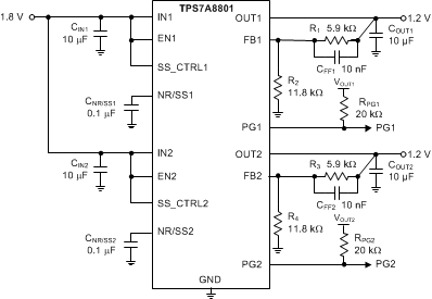
This section discusses the implementation of the TPS7A88 to regulate from a common input voltage to two output voltages of the same value. This is a common application where two noise-sensitive loads must have the same supply voltage but have high channel-to-channel isolation. The schematic for this application circuit is provided in Figure 43.
 Figure 43. Application Example
8.2.1 Design Requirements
For the design example shown in Figure 43, use the parameters listed in Table 3 as the input parameters.
Table 3. Design Parameters
| PARAMETER | DESIGN REQUIREMENT |
|---|---|
| Input voltages (VIN1 and VIN2) | 1.8 V, ±3%, provided by the dc-dc converter switching at 750 kHz |
| Maximum ambient operating temperature | 55°C |
| Output voltages (VOUT1 and VOUT2) | 1.2 V, ±1%, output voltages are isolated |
| Output currents (IOUT2 and IOUT2) | 1.0 A (maximum), 10 mA (minimum) |
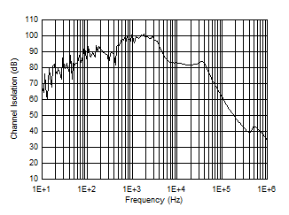
| Channel-to-channel isolation | Isolation greater than 50 dB at 100 kHz |
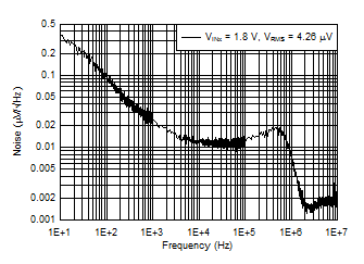
| RMS noise | < 5 µVRMS, bandwidth = 10 Hz to 100 kHz |
| PSRR at 750 kHz | > 40 dB |
| Startup time | < 5 ms |
8.2.2 Detailed Design Procedure
The output voltages can be set to 1.2 V by selecting the correct values for R1, R3 and R2, R4; see Equation 2.
Input and output capacitors are selected in accordance with the Capacitor Recommendation section. Ceramic capacitances of 10 µF for both inputs and outputs are selected.
To satisfy the required startup time (tSSx) and still maintain low-noise performance, a 0.1-µF CNR/SSx is selected for both channels with SS_CTRL1 and SS_CTRL2 connected to VIN1 and VIN2, respectively. This value is calculated with Equation 9.
With a 1.0-A maximum load, the internal power dissipation is 600 mW per channel or 1.2 W total, which corresponds to a 40°C junction temperature rise. With an 55°C maximum ambient temperature, the junction temperature is at 95°C. To minimize noise, a feed-forward capacitance (CFF) of 10 nF is selected.
Channel-to-channel isolation depends greatly on the layout of the design. To minimize crosstalk between the outputs, keep the output capacitor grounds on separate sides of the design. See the Layout section for an example of how to layout the TPS7A88 to achieve best PSRR, channel-to-channel isolation, and noise.
8.2.3 Application Curves


8.3 Do's and Don'ts
Table 4 lists the recommended guidelines for the TPS7A88.
Table 4. Recommended Guidelines for Designing with the TPS7A88
| DO'S | DON'TS |
|---|---|
| Do place at least one 10-µF ceramic capacitor as close as possible to each output of the device. | Do not place either output capacitor more than 10 mm away from the regulator. |
| Do connect a 10-μF or larger low equivalent series resistance (ESR) capacitor across each input pin to GND. | Do not exceed the absolute maximum ratings. |
| Do follow the recommended layout in Figure 47 | Do not leave the enable pins floating. |