SLVSCB2D October   2013  – April 2018

PRODUCTION DATA.  

  1. Features
  2. Applications
  3. Description
    1.     Device Images
      1.      Adjustable Output Option
      2.      Fixed Output Option
  4. Revision History
  5. Device Comparison
  6. Pin Configuration and Functions
    1.     Pin Functions
  7. Specifications
    1. 7.1 Absolute Maximum Ratings
    2. 7.2 ESD Ratings
    3. 7.3 Recommended Operating Conditions
    4. 7.4 Thermal Information
    5. 7.5 Electrical Characteristics
    6. 7.6 Timing Requirements
    7. 7.7 Typical Characteristics
  8. Detailed Description
    1. 8.1 Overview
    2. 8.2 Functional Block Diagrams
    3. 8.3 Feature Description
      1. 8.3.1 Enable (EN)
      2. 8.3.2 Regulated Output (VOUT)
      3. 8.3.3 Power-On-Reset (RESET)
      4. 8.3.4 Reset Delay Timer (DELAY)
      5. 8.3.5 Adjustable Output Voltage (ADJ for TPS7B6701)
      6. 8.3.6 Undervoltage Shutdown
      7. 8.3.7 Thermal Shutdown
      8. 8.3.8 Thermal Protection
    4. 8.4 Device Functional Modes
      1. 8.4.1 Operation With VIN < 4 V
      2. 8.4.2 Operation With EN Control
  9. Application and Implementation
    1. 9.1 Application Information
    2. 9.2 Typical Application
      1. 9.2.1 Design Requirements
      2. 9.2.2 Detailed Design Procedure
        1. 9.2.2.1 Power Dissipation and Thermal Considerations
      3. 9.2.3 Application Curves
  10. 10Power Supply Recommendations
    1. 10.1 Dropout Recovery
      1. 10.1.1 LDO Dropout Recovery Explained
      2. 10.1.2 TPS7B67xx-Q1 Dropout During Startup
  11. 11Layout
    1. 11.1 Layout Guidelines
      1. 11.1.1 Enhanced Thermal Pad
      2. 11.1.2 Package Mounting
      3. 11.1.3 Board Layout Recommendations to Improve PSRR and Noise Performance
      4. 11.1.4 Additional Layout Considerations
    2. 11.2 Layout Example
  12. 12Device and Documentation Support
    1. 12.1 Related Links
    2. 12.2 Receiving Notification of Documentation Updates
    3. 12.3 Community Resources
    4. 12.4 Trademarks
    5. 12.5 Electrostatic Discharge Caution
    6. 12.6 Glossary
  13. 13Mechanical, Packaging, and Orderable Information

Package Options

Mechanical Data (Package|Pins)
Thermal pad, mechanical data (Package|Pins)
Orderable Information

Pin Configuration and Functions

PWP Package
20-Pin HTSSOP With PowerPAD™
Top View
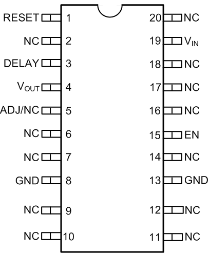
TPS7B6701-Q1 TPS7B6733-Q1 TPS7B6750-Q1 pwp_slvscb2.gif

Pin Functions

PIN TYPE DESCRIPTION
NAME PWP
ADJ 5 I Feedback pin. This pin is used with an external resistor divider or the NC pin when in a fixed version.
DELAY 3 O Reset pulse delay adjustment. Connect this pin through a capacitor to GND.
EN 15 I Enable pin. When the EN pin becomes lower than threshold, the device enters the stand-by state.
GND 8, 13 G Ground reference
NC 2, 6, 7, 9, 10, 11, 12, 14, 16, 17, 18, 20 Not connected
RESET 1 O Output ready. This open-drain pin must be connected to VOUT through an external resistor. RESET is pulled down when the output voltage goes below threshold.
VIN 19 P Input power-supply voltage
VOUT 4 P Output voltage
PowerPAD™ Thermal pad