SLVSCB2D October   2013  – April 2018

PRODUCTION DATA.  

  1. Features
  2. Applications
  3. Description
    1.     Device Images
      1.      Adjustable Output Option
      2.      Fixed Output Option
  4. Revision History
  5. Device Comparison
  6. Pin Configuration and Functions
    1.     Pin Functions
  7. Specifications
    1. 7.1 Absolute Maximum Ratings
    2. 7.2 ESD Ratings
    3. 7.3 Recommended Operating Conditions
    4. 7.4 Thermal Information
    5. 7.5 Electrical Characteristics
    6. 7.6 Timing Requirements
    7. 7.7 Typical Characteristics
  8. Detailed Description
    1. 8.1 Overview
    2. 8.2 Functional Block Diagrams
    3. 8.3 Feature Description
      1. 8.3.1 Enable (EN)
      2. 8.3.2 Regulated Output (VOUT)
      3. 8.3.3 Power-On-Reset (RESET)
      4. 8.3.4 Reset Delay Timer (DELAY)
      5. 8.3.5 Adjustable Output Voltage (ADJ for TPS7B6701)
      6. 8.3.6 Undervoltage Shutdown
      7. 8.3.7 Thermal Shutdown
      8. 8.3.8 Thermal Protection
    4. 8.4 Device Functional Modes
      1. 8.4.1 Operation With VIN < 4 V
      2. 8.4.2 Operation With EN Control
  9. Application and Implementation
    1. 9.1 Application Information
    2. 9.2 Typical Application
      1. 9.2.1 Design Requirements
      2. 9.2.2 Detailed Design Procedure
        1. 9.2.2.1 Power Dissipation and Thermal Considerations
      3. 9.2.3 Application Curves
  10. 10Power Supply Recommendations
    1. 10.1 Dropout Recovery
      1. 10.1.1 LDO Dropout Recovery Explained
      2. 10.1.2 TPS7B67xx-Q1 Dropout During Startup
  11. 11Layout
    1. 11.1 Layout Guidelines
      1. 11.1.1 Enhanced Thermal Pad
      2. 11.1.2 Package Mounting
      3. 11.1.3 Board Layout Recommendations to Improve PSRR and Noise Performance
      4. 11.1.4 Additional Layout Considerations
    2. 11.2 Layout Example
  12. 12Device and Documentation Support
    1. 12.1 Related Links
    2. 12.2 Receiving Notification of Documentation Updates
    3. 12.3 Community Resources
    4. 12.4 Trademarks
    5. 12.5 Electrostatic Discharge Caution
    6. 12.6 Glossary
  13. 13Mechanical, Packaging, and Orderable Information

Package Options

Mechanical Data (Package|Pins)
Thermal pad, mechanical data (Package|Pins)
Orderable Information

Reset Delay Timer (DELAY)

An external capacitor on this pin sets the timer delay before the reset pin is asserted high. The constant output current charges an external capacitor until the voltage exceeds a threshold to trip an internal comparator. If this pin is open, the default delay time is 325 µs (typical).

The reset pulse delay time td, is defined with the charge time of an external capacitor DELAY (see Equation 1).

Equation 1. TPS7B6701-Q1 TPS7B6733-Q1 TPS7B6750-Q1 eq_1_delay_slvscb2.gif

The power-on-reset initializes when VO exceeds 91.6% of the programmed value. The power-on-reset delay is a function of the value set by an external capacitor on the DELAY pin before the RESET pin is released high.
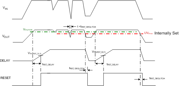
TPS7B6701-Q1 TPS7B6733-Q1 TPS7B6750-Q1 timing_reset_slvscb2.gifFigure 18. Conditions to Activate RESET
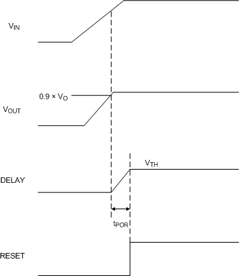
TPS7B6701-Q1 TPS7B6733-Q1 TPS7B6750-Q1 timing_delay_slvscb2.gifFigure 19. External Programmable-Reset Delay