SBVS402 April 2020 TPS7B81
PRODUCTION DATA.
- 1 Features
- 2 Applications
- 3 Description
- 4 Revision History
- 5 Pin Configuration and Functions
- 6 Specifications
- 7 Detailed Description
- 8 Application and Implementation
- 9 Power Supply Recommendations
- 10Layout
- 11Device and Documentation Support
- 12Mechanical, Packaging, and Orderable Information
Package Options
Mechanical Data (Package|Pins)
Thermal pad, mechanical data (Package|Pins)
Orderable Information
8.1.1 Power Dissipation
Circuit reliability demands that proper consideration is given to device power dissipation, location of the circuit on the printed circuit board (PCB), and correct sizing of the thermal plane. The PCB area around the regulator must be as free as possible of other heat-generating devices that cause added thermal stresses.
As a first-order approximation, power dissipation in the regulator depends on the input-to-output voltage difference and load conditions. Equation 1 approximates PD:
An important note is that power dissipation can be minimized, and thus greater efficiency achieved, by proper selection of the system voltage rails. Proper selection allows the minimum input-to-output voltage differential to be obtained. The low dropout of the device allows for maximum efficiency across a wide range of output voltages.
The main heat conduction path for the device is through the thermal pad on the package. As such, the thermal pad must be soldered to a copper pad area under the device. This pad area contains an array of plated vias that conduct heat to any inner plane areas or to a bottom-side copper plane.
The maximum power dissipation determines the maximum allowable junction temperature (TJ) for the device. According to Equation 2, power dissipation and junction temperature are most often related by the junction-to-ambient thermal resistance (RθJA) of the combined PCB, device package, and the temperature of the ambient air (TA). This equation is rearranged for output current in Equation 3.
Unfortunately, this thermal resistance (RθJA) is highly dependent on the heat-spreading capability built into the particular PCB design, and therefore varies according to the total copper area, copper weight, and location of the planes. The RθJA recorded in the Thermal Information table is determined by the JEDEC standard, PCB, and copper-spreading area, and is only used as a relative measure of package thermal performance. For a well-designed thermal layout, RθJA is actually the sum of the package junction-to-case (bottom) thermal resistance (RθJCbot) plus the thermal resistance contribution by the PCB copper.
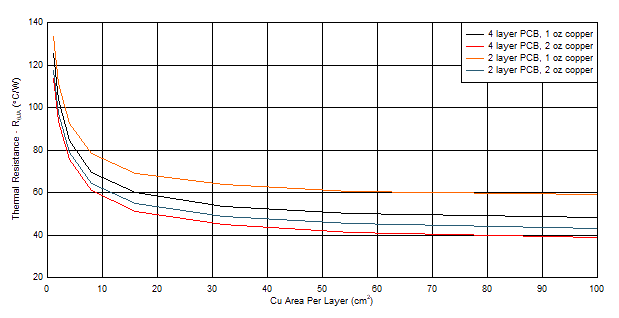
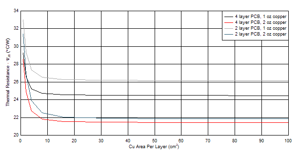
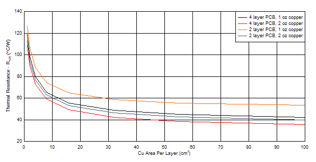
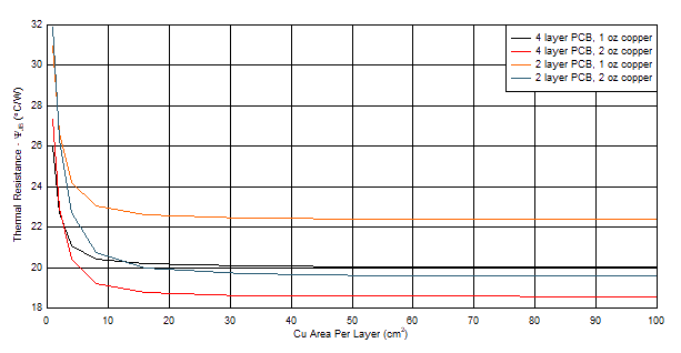
Figure 25 through Figure 28 illustrate the functions of RθJA and ψJB versus copper area and thickness. These plots are generated with a 101.6-mm x 101.6-mm x 1.6-mm PCB of two and four layers. For the four-layer board, inner planes use a 1-oz copper thickness. Outer layers are simulated with both 1-oz and 2-oz copper thicknesses. A 2 x 1 array of thermal vias with a 300-µm drill diameter and a 25-µm copper (Cu) plating is located beneath the thermal pad of the device. The thermal vias connect the top layer, the bottom layer and, in the case of the 4-layer board, the first inner GND plane. The copper plane of each layer is of an equal area.
 Figure 25. RθJA versus Cu Area for the WSON (DRV) Package
  Figure 26. ψJB versus Cu Area for the WSON (DRV) Package
  Figure 27. RθJA versus Cu Area for the HVSSOP (DGN) Package
  Figure 28. ψJB versus Cu Area for the HVSSOP (DGN) Package