SLVSGX6B February 2023 – December 2023 TPS7H3302-SEP , TPS7H3302-SP
PRODUCTION DATA
- 1
- 1 Features
- 2 Applications
- 3 Description
- 4 Device Options
- 5 Pin Configuration and Functions
- 6 Specifications
- 7 Detailed Description
-
8 Application and Implementation
- 8.1 Application Information
- 8.2
Typical Application
- 8.2.1 Design Requirements
- 8.2.2
Detailed Design Procedure
- 8.2.2.1 VDD Capacitor
- 8.2.2.2 VLDO Input Capacitor
- 8.2.2.3 VTT Output Capacitor
- 8.2.2.4 VTTSNS Connection
- 8.2.2.5 Low VDD Applications
- 8.2.2.6 S3 and Pseudo-S5 Support
- 8.2.2.7 Tracking Startup and Shutdown
- 8.2.2.8 Output Tolerance Consideration for VTT DIMM or Module Applications
- 8.2.2.9 LDO Design Guidelines
- 8.2.3 Application Curve
- 8.3 Power Supply Recommendations
- 8.4 Layout
- 9 Device and Documentation Support
- 10Revision History
- 11Mechanical, Packaging, and Orderable Information
Package Options
Refer to the PDF data sheet for device specific package drawings
Mechanical Data (Package|Pins)
- DAP|32
Thermal pad, mechanical data (Package|Pins)
- DAP|32
Orderable Information
8.2.2.8 Output Tolerance Consideration for VTT DIMM or Module Applications
The TPS7H3302 is specifically designed to power up the memory termination rail (as shown in Figure 8-5). The DDR memory termination structure determines the main characteristics of the VTT rail, which is to be able to sink and source current while maintaining acceptable VTT tolerance. See Figure 8-6 for typical characteristics for a single memory cell.
 Figure 8-5 Typical Application Diagram for DDR3 VTT DIMM/Module Using TPS7H3302
In Figure 8-6, when Q1 is on and Q2 is off:
- Current flows from VDDQ via the termination resistor to VTT.
- VTT sinks current.
In Figure 8-6, when Q2 is on and Q1 is off:
- Current flows from VTT via the termination resistor to GND.
- VTT sources current.
 Figure 8-6 DDR Physical
Signal System SSTL Signaling
Figure 8-6 DDR Physical
Signal System SSTL SignalingBecause VTT accuracy has a direct impact on the memory signal integrity, it is imperative to understand the tolerance requirement on VTT. Based on JEDEC VTT specifications for DDR and DDR2. See Table 8-2 for detailed information and JEDEC relevant specifications.
VTTREF – 40 mV < VTT < VTTREF + 40 mV, for both DC and AC conditions
The specification itself indicates that VTT must keep track of VTTREF for proper signal conditioning.
The TPS7H3302 specifies the regulator output voltage to be:
VTTREF – 30 mV < VTT < VTTREF + 30 mV, for both DC and AC conditions and –3 A < IVTT < 3 A.
The regulator output voltage is measured at the regulator side, not the load side. The tolerance is applicable to DDR, DDR2, DDR3 and low-power DDR3/DDR4 applications (see Table 8-2 for detailed information). To meet the stability requirement, a minimum output capacitance of 470 μF is needed, combination of both tantalum and ceramic capacitors. Considering the actual tolerance on the MLCC capacitors, four 4.7-μF ceramic capacitors in parallel with 3 × 150-µF low-ESR tantalum capacitor are sufficient to meet the above requirement. Higher ESR tantalum capacitors will require multiple tantalum capacitors in parallel with ceramic capacitors to meet system needs.
| DDR | DDR2 | DDR3 | LOW POWER DDR3 (DDR3L) | |||
|---|---|---|---|---|---|---|
| FSB data rates | 200, 266, 333 and 400 MHz | 400, 533, 677 and 800 MHz | 800, 1066, 1330 and 1600 MHz | Same as DDR3 | ||
| Termination | Motherboard termination to VTT for all signals | On-die termination for data group. VTT used for termination of address, command and control signals. | On-die termination for data group. VTT used for termination of address, command and control signals. | Same as DDR3 | ||
| Termination current demand | Max sink and source transient currents of up to 2.6 A to 2.9 A |
Not as demanding
|
Not as demanding
|
Same as DDR3 | ||
| Voltage level | 2.5-V core and I/O 1.25-V VTT | 1.8-V core and I/O 0.9-V VTT | 1.5-V core and I/O 0.75-V VTT | 1.35-V core and I/O 0.68-V VTT | ||
| Relevant JEDEC specification | JESD79F (SSTL_2 JESD8-9B) | DDR2 JESD79-2F (SSTL_18 JESD8-15) | DDR3 JESD79-3F | DDR3L JESD79-3-1A.01 | ||
The TPS7H3302 is designed as a Gm-driven LDO. The voltage droop between the reference input and the output regulator is determined by the transconductance and output current of the device. The typical Gm is 250 S at 3 A and changes with respect to the load in order to conserve the quiescent current (that is, the Gm is very low at no load condition). The Gm LDO regulator is a single pole system. Its unity gain bandwidth for the voltage loop is only determined by the output capacitance, as a result of the bandwidth nature of the Gm. (See Equation 1)
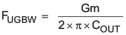
where
- FUGBW is the unity gain bandwidth
- Gm is transconductance
- COUT is the output capacitance
There are two limitations to this type of regulator when it comes to the output bulk capacitor requirement. To maintain stability, the zero location contributed by the ESR of the output capacitors should be greater than the –3-dB point of the current loop. This constraint means that higher ESR capacitors should not be used in the design. In addition, the impedance characteristics of the ceramic capacitor should be well understood in order to prevent the gain peaking effect around the Gm –3-dB point because of the large ESL, the output capacitor, and parasitic inductance of the VTT trace.
Figure 8-7 shows the bode plot simulation for a typical DDR3 configuration of the TPS7H3302, where:
- VDD = 2.4 V
- VVLDOIN = 1.5 V
- VTT = 0.75 V
- IIO = 3 A
- 3 × 150-μF low-ESR tantalum capacitors (T530D157M010ATE005) in parallel with 4 × 4.7-µF ceramic capacitor
- ESR = 1.66 mΩ
- ESL = 800 pH
The unity-gain bandwidth is approximately 85 kHz and the phase margin is 92°. The 0-dB level is crossed, the gain peaks because of the ESL effect. However, the peaking is kept well below 0 dB.
 Figure 8-7 Bode Plot for a
Typical DDR3 Configuration
Figure 8-7 Bode Plot for a
Typical DDR3 ConfigurationThe figure below shows the Load Regulation and Transient Plot shows the transient response for a typical DDR3 configuration. When the regulator is subjected to a ±1.875-A load step. The current shown only represents the device sourcing 1.875 A due to location of current probe.
 Figure 8-8 Transient
Plot
Figure 8-8 Transient
Plot