SLVSGG1A February 2022 – September 2022 TPS7H5005-SEP , TPS7H5006-SEP , TPS7H5007-SEP , TPS7H5008-SEP
PRODUCTION DATA
- 1 Features
- 2 Applications
- 3 Description
- 4 Revision History
- 5 Device Comparison Table
- 6 Pin Configuration and Functions
-
7 Specifications
- 7.1 Absolute Maximum Ratings
- 7.2 ESD Ratings
- 7.3 Recommended Operating Conditions
- 7.4 Thermal Information
- 7.5 Electrical Characteristics: All Devices
- 7.6 Electrical Characteristics: TPS7H5005-SEP
- 7.7 Electrical Characteristics: TPS7H5006-SEP
- 7.8 Electrical Characteristics: TPS7H5007-SEP
- 7.9 Electrical Characteristics: TPS7H5008-SEP
- 7.10 Typical Characteristics
-
8 Detailed Description
- 8.1 Overview
- 8.2 Functional Block Diagram
- 8.3
Feature Description
- 8.3.1 VIN and VLDO
- 8.3.2 Start-Up
- 8.3.3 Enable and Undervoltage Lockout (UVLO)
- 8.3.4 Voltage Reference
- 8.3.5 Error Amplifier
- 8.3.6 Output Voltage Programming
- 8.3.7 Soft Start (SS)
- 8.3.8 Switching Frequency and External Synchronization
- 8.3.9 Primary Switching Outputs (OUTA/OUTB)
- 8.3.10 Synchronous Rectifier Outputs (SRA/SRB)
- 8.3.11 Dead Time and Leading Edge Blank Time Programmability (PS, SP, and LEB)
- 8.3.12 Pulse Skipping
- 8.3.13 Duty Cycle Programmability
- 8.3.14 Current Sense and PWM Generation (CS_ILIM)
- 8.3.15 Hiccup Mode Operation (HICC)
- 8.3.16 External Fault Protection (FAULT)
- 8.3.17 Slope Compensation (RSC)
- 8.3.18 Frequency Compensation
- 8.3.19 Thermal Shutdown
- 8.4 Device Functional Modes
-
9 Application and Implementation
- 9.1 Application Information
- 9.2
Typical Application
- 9.2.1 Design Requirements
- 9.2.2
Detailed Design Procedure
- 9.2.2.1 Switching Frequency
- 9.2.2.2 Output Voltage Programming Resistors
- 9.2.2.3 Dead Time
- 9.2.2.4 Leading Edge Blank Time
- 9.2.2.5 Soft-Start Capacitor
- 9.2.2.6 Transformer
- 9.2.2.7 Main Switching FETs
- 9.2.2.8 Synchronous Rectificier FETs
- 9.2.2.9 RCD Clamp
- 9.2.2.10 Output Inductor
- 9.2.2.11 Output Capacitance and Filter
- 9.2.2.12 Sense Resistor
- 9.2.2.13 Hiccup Capacitor
- 9.2.2.14 Frequency Compensation Components
- 9.2.2.15 Slope Compensation Resistor
- 10Power Supply Recommendations
- 11Layout
- 12Device and Documentation Support
- 13Mechanical, Packaging, and Orderable Information
Package Options
Mechanical Data (Package|Pins)
- PW|24
Thermal pad, mechanical data (Package|Pins)
Orderable Information
8.3.11 Dead Time and Leading Edge Blank Time Programmability (PS, SP, and LEB)
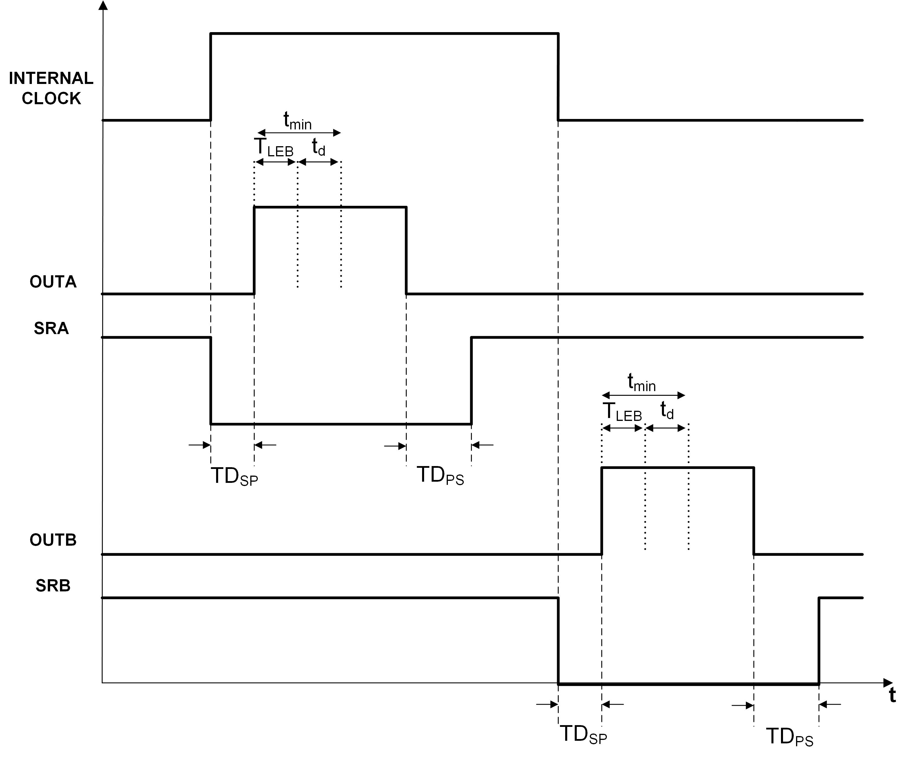
While the TPS7H5007-SEP has a fixed dead time (50 ns typical), the TPS7H5005-SEP and TPS7H5006-SEP allow for the user to program two independent dead times, TDSP and TDPS, as shown in Figure 8-13. This allows for the dead times to be optimized by the user in order to prevent shoot-though between the primary and synchronous switches while attaining the best possible converter efficiency. Table 8-4 shows the dead time configurations for each device. The dead time TDPS between primary output (OUTA/OUTB) turn-off to synchronous rectifier (SRA/SRB) turn-on, can be programmed using a resistor from PS to AVSS. Likewise, the dead time TDSP between synchronous rectifier turn-off and primary output turn-on is set using a resistor from SP to AVSS. The equation for determining the values of RPS and RSP required for a desired dead time is shown in Equation 8.
where:
- DT is the desired dead time in ns
- RPS and RSP are in kΩ
If the PS and SP pins are left floating, the dead time will be set to a minimum value of 8 ns (typical). When these pins are populated, it is recommended to use a minimum resistor value of 10 kΩ for RPS and RSP. The maximum resistor value to be used is 300 kΩ. As mentioned in Soft-Start (SS) and Synchronous Rectifier Outputs (SRA/SRB), the SR outputs will be disabled during soft start, so the dead time is observed only after this sequence is complete.
After OUTA or OUTB goes high, a leading edge blank time is implemented to remove any transient noise from the current sensing loop. While the leading edge blank time is fixed (50 ns typical) for TPS7H5007-SEP, the leading edge blank time for all other devices in the TPS7H500x-SEP series is programmable by placing an external resistor from LEB to AVSS. This pin cannot be left floating for the programmable devices and a minimum resistor value of 10 kΩ is required from LEB to AVSS. The maximum resistor value that should be used is 300 kΩ. The equation for determining the value of RLEB for a desired leading edge blank time is shown in Equation 9.
where:
- LEB is the desired leading edge blank time in ns
- RLEB is in kΩ
| DEVICE | DEAD TIME | LEADING EDGE BLANK TIME |
|---|---|---|
| TPS7H5005-SEP | Resistor programmable | Resistor programmable |
| TPS7H5006-SEP | Resistor programmable | Resistor programmable |
| TPS7H5007-SEP | Fixed (50-ns typical) | Fixed (50-ns typical) |
| TPS7H5008-SEP | Not applicable | Resistor programmable |
In Figure 8-13, the dead times and leading edge blank times are shown for the switching waveforms. This figure also illustrates the minimum on-time of the device, which is comprised of the programmed blank time TLEB and an internal logic delay td. Note that the dead-time waveforms for OUTB/SRB are only applicable for TPS7H5005-SEP.
 Figure 8-13 Outputs
Timing Waveforms